NanoWorld AG CEO Manfred Detterbeck is attending NANOKOREA 2024, the 22nd International #Nanotech Symposium & Exhibition on nanoscale science and technology , which will be held from July 3-5, 2024 at KINTEX (Korea International Exhibition Center), Goyang-si, Gyeonggi-do, South Korea. http://www.nanokorea-sympo.or.kr/welcome.php
This year’s main theme is: Invisible Nano Realizes the Future
Will we meet you there too?
Manfred Detterbeck is already looking forward to Nano Korea 2024. See you there!
The ability to maximize the range of exciton transport while minimizing energy loss has significant implications for the design of future nanoscale light harvesting, optoelectronic, and sensing applications. *
One method of achieving this would be to densely pack dyes into strongly coupled aggregates such that excitations can be coherently delocalized through the partial or full length of the aggregate. *
Coherently coupled aggregates enable exciton migration over discreet spatial distances with near unitary quantum efficiency. As a result, controlled dye aggregation has long been studied by chemists as a method of tuning the photonic and physical properties of the dyes and pigments in light harvesting devices. An example of this coherent coupling phenomenon can be observed in the cyanine dye family and specifically the prototypical example, pseudoisocyanine (PIC) dye. *
In the article «Structural and optical variation of pseudoisocyanine aggregates nucleated on DNA substrates” Matthew Chiriboga, Christopher M Green, Divita Mathur, David A Hastman, Joseph S Melinger, Remi Veneziano, Igor L Medintz and Sebastián A Díaz show that DNA-nucleated PIC aggregates have properties which correlate to different molecular structures and are directed by changing the DNA scaffold. *
To achieve this, they formed PIC aggregates through heterogeneous nucleation by mixing dissolved PIC dye with various DNA nanostructures ranging from a rigid DX-tile to more flexible DNA duplex (dsDNA) or single strand DNA oligonucleotide (ssDNA). *
Although the aggregates Matthew Chiriboga et al formed required elevated excess of PIC dye relative to previously reported J-bits, they exhibited sharper and brighter fluorescence peaks as well as longer Ncoh. *
Therefore, the authors refer to aggregates formed by this approach as super aggregate (SA) in their article, though they note SA formed with different DNA substrates result in unique properties. *
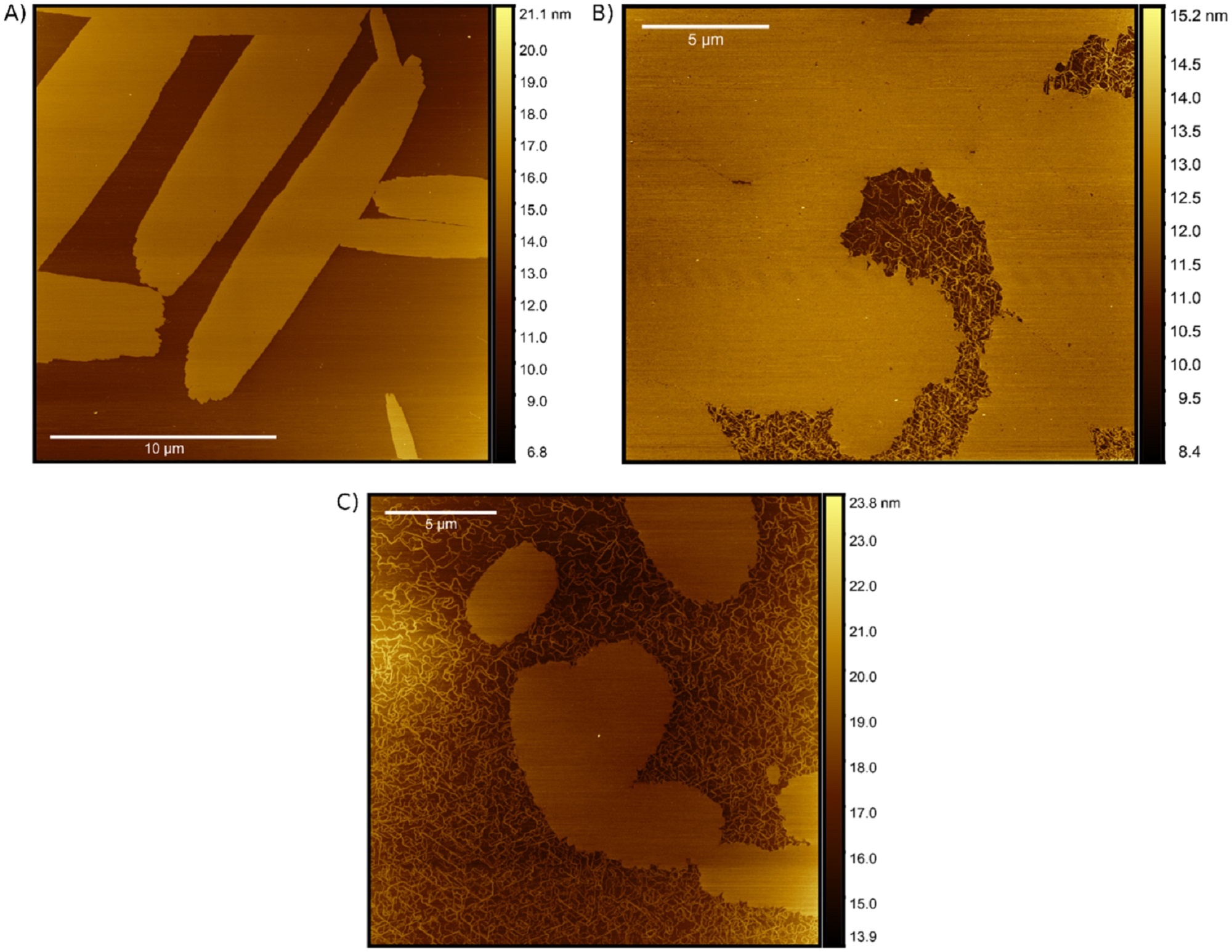
Complementary circular dichroism (CD) and atomic force microscopy (AFM) characterizations were used to analyze the SA and both indicated distinctions in the way each substrate and subsequent dye aggregate incorporates the individual PIC molecules. *
To achieve high resolution imaging of nucleic acid nanostructures, the DNA is often deposited onto a mica substrate, where mica electrostatically binds the DNA. Once deposited onto the mica, the imaging can be done in a hydrated environment as there is no additional required dehydration or staining of the DNA, a particularly convenient advantage of AFM. *
On a segment of freshly cleaved mica mounted to a magnetic puck, 15 μl of PIC-DANN solution was deposited immediately before measurement. A 25 μl droplet of imaging buffer was deposited on the AFM tip, then the AFM tip mount was lowered into the sample buffer to create a liquid ‘chamber’ for imaging. *
When introducing various DNA scaffolds for SA formation and subsequent AFM imaging, Matthew Chiriboga et al. observed significant changes in the aggregates structure. *
The AFM imaging highlighted the stark differences in aggregate formation resulting from the DNA substrates. *
To the author’s knowledge this is the first visualization of DNA-based PIC aggregates. Results from the field have been pointing towards fiber-like or nanotube-like networks of polymerized PIC as a structural model for aggregates suspended in solution. *
On the other hand, other AFM studies demonstrate that PIC aggregates formed on mica substrates adopt a leafy island morphology. *
Interestingly, Matthew Chiriboga et al. observe evidence of both PIC fibers as well as leafy islands that exhibit distinct growth patterns, again depending on the DNA substrate. *
Although this work contributes to the growing body of evidence that solution-based PIC aggregates form fibrous networks structures, the AFM measurements presented in the article highlight the multiplicity of PIC aggregation modes when introduced to DNA scaffolds. *
The results presented in the research article suggest modification of the DNA substrate results in significant changes to how the DNA and companion dye molecules are integrated into larger form PIC aggregates. *
Bearing in mind that the broader motivation for studying DNA based PIC aggregates is to integrate strongly coupled dyes onto modular DNA structural units, PIC SAs should be given due consideration as a versatile option. *
In fact, similar work is being done with other cyanine dyes where DNA template modification is used to switch between quenching and energy transfer. *
Ultimately this could be a path for the PIC SA and one which possibly leads towards applications in optical microcavities for quantum electrodynamical devices and optical switching, molecular plasmonics, biosensors, and light-harvesting arrays. *
Figure 6 from Matthew Chiriboga et al. “Structural and optical variation of pseudoisocyanine aggregates nucleated on DNA substrates”: AFM visualization of SA formations. AFM visualizations of PIC aggregates formed in the (A) AT, (B) dsDNA, and (C) ssDNA nanostructures. Each of the samples was formed immediately before measurement by mixing 160 μM PIC dye with 500 nM DNA normalized to the dye-labeled strand concentration (i.e. 320-fold excess).
*Matthew Chiriboga, Christopher M Green, Divita Mathur, David A Hastman, Joseph S Melinger, Remi Veneziano, Igor L Medintz and Sebastián A Díaz Structural and optical variation of pseudoisocyanine aggregates nucleated on DNA substrates
Methods and Applications in Fluorescence (2023) 11 014003
DOI: https://doi.org/10.1088/2050-6120/acb2b4
The article “Active self-assembly of piezoelectric biomolecular films via synergistic nanoconfinement and in-situ poling” by Matthew Chiriboga, Christopher M Green, Divita Mathur, David A Hastman, Joseph S Melinger, Remi Veneziano, Igor L Medintz and Sebastián A Díaz is licensed under a Creative Commons Attribution 4.0 International License, which permits use, sharing, adaptation, distribution and reproduction in any medium or format, as long as you give appropriate credit to the original author(s) and the source, provide a link to the Creative Commons license, and indicate if changes were made. The images or other third-party material in this article are included in the article’s Creative Commons license, unless indicated otherwise in a credit line to the material. If material is not included in the article’s Creative Commons license and your intended use is not permitted by statutory regulation or exceeds the permitted use, you will need to obtain permission directly from the copyright holder. To view a copy of this license, visit https://creativecommons.org/licenses/by/4.0/.
Over several decades many studies on the reduction of wear of mechanical systems have been conducted.
Methods to reduce wear are generally divided into the following categories: applying lubrication, coating with high-hardness materials, and surface texturing. *
Several studies have reported that coatings with higher hardness show more wear than those with lower hardness. From these reports, it is apparent that wear does not depend solely on the hardness of the surface. Hence, there is a strong motivation for utilizing additional strategies for designing wear-resistive surfaces rather than only enhancing the hardness of the coating. *
In the article “Feasibility of wear reduction for soft nanostructured thin film through enhanced elastic recoverability and contact stress relief” Kuk-Jin Seo, Hyun-Joon Kim and Dae-Eun Kim show, that a soft, thin film comprising randomly aligned carbon nanotubes (CNTs) can reduce surface wear more effectively than a homogeneous thin film because of enhanced elastic recoverability and contact stress relief originating from its mesh structure. *
To investigate the wear characteristics of the mesh structure compared to those of the homogeneous thin film, multi-walled CNTs (MWCNTs) and diamond-like carbon (DLC) thin films were prepared to conduct nanoscale tribological experiments using atomic force microscopy (AFM). The MWCNT thin film showed unmeasurably low wear compared with the DLC thin film under a certain range of normal load. *
To demonstrate the wear reduction mechanism of the MWCNT thin film, its indentation and frictional behaviors were assessed. The indentation behavior of the MWCNT thin film revealed repetitive elastic deformation with a wide strain range and a significantly lower elastic modulus than that of the DLC thin film. The permanent deformation of the MWCNT thin film was observed through frictional experiments under relatively high normal load conditions. *
The presented results are expected to provide insights into the design of highly wear-resistant surfaces using nanostructures. *
The thickness and surface roughness of the MWCNT and DL thin films were measured using Atomic Force Microscopy. *
The force-displacement (F-D) curves were measured on the MWCNT thin film using the AFM to verify the mechanical behavior when indented by the zirconia microspheres that were used for wear and friction experiments. *
The adhesion forces between the thin films and zirconia microspheres were measured by observing the pull-off force of the F-D curve with the AFM. *
The adhesion force was measured using a colloidal AFM probe to aid the analysis of the tribological characteristics of the thin film. *
The pull-off forces for the DL specimens were obtained at 35 different locations with displacements of 50-200 nm. *
Diamond-coated AFM probes (NanoWorld Pointprobe® DT-NCHR ) were used for scanning, while non-coated silicon AFM probes with relatively high and low spring constants (NanoWorld Pointprobe®NCHR and CONTR) were used for the tribological experiments and specimen characterizations. *
Figure 6 from “Feasibility of wear reduction for soft nanostructured thin film through enhanced elastic recoverability and contact stress relief” by Kuk-Jin Seo et al.: AFM images of wear tracks on the MWCNT thin film under test conditions of (a) 2,000 nN and 20,000 cycles, (b) 6,000 nN and 30,000 cycles, (c) 7,000 nN and 30,000 cycles, (d) 9,200 nN and 30,000 cycles, (e) 13,500 nN and 30,000 cycles, and (f) 28,000 nN and 30,000 cycles. Post-processed AFM images that subtracted the original image before each wear test under conditions of (g) 6,000 nN and 30,000 cycles, (h) 7,000 nN and 30,000 cycles, and (i) 28,000 nN and 30,000 cycles
*Kuk-Jin Seo, Hyun-Joon Kim and Dae-Eun Kim Feasibility of wear reduction for soft nanostructured thin film through enhanced elastic recoverability and contact stress relief
Friction 11(7): 1292-1306 (2023)
DOI: https://doi.org/10.1007/s40544-022-0669-7
The article “Feasibility of wear reduction for soft nanostructured thin film through enhanced elastic recoverability and contact stress relief” by Kuk-Jin Seo, Hyun-Joon Kim and Dae-Eun Kim is licensed under a Creative Commons Attribution 4.0 International License, which permits use, sharing, adaptation, distribution and reproduction in any medium or format, as long as you give appropriate credit to the original author(s) and the source, provide a link to the Creative Commons license, and indicate if changes were made. The images or other third-party material in this article are included in the article’s Creative Commons license, unless indicated otherwise in a credit line to the material. If material is not included in the article’s Creative Commons license and your intended use is not permitted by statutory regulation or exceeds the permitted use, you will need to obtain permission directly from the copyright holder. To view a copy of this license, visit https://creativecommons.org/licenses/by/4.0/.