Detecting Early-Stage Cohesion Due to Calcium Silicate Hydration with Rheology and Surface Force Apparatus

Extremely robust cohesion triggered by calcium silicate hydrate (C–S–H) precipitation during cement hardening makes concrete one of the most commonly used man-made materials. *

In the article “Detecting Early-Stage Cohesion Due to Calcium Silicate Hydration with Rheology and Surface Force Apparatus” Teresa Liberto, Andreas Nenning, Maurizio Bellotto, Maria Chiara Dalconi, Dominik Dworschak, Lukas Kalchgruber, Agathe Robisson, Markus Valtiner and Joanna Dziadkowiec present a proof-of-concept study, in which they seek an additional nanoscale understanding of early-stage cohesive forces acting between hydrating model tricalcium silicate (C3S) surfaces by combining rheological and surface force measurements. *

The composition and surface properties of the PLD-deposited calcium silicate films have been analyzed by X-ray diffraction (XRD), X-ray photoelectron spectroscopy (XPS), scanning electron microscopy with energy-dispersive spectroscopy (SEM-EDS), and atomic force microscopy (AFM). *

The calcium silicate surfaces were initially scanned in air. Subsequently, the authors injected about 1 mL of MilliQ water on top of the films so that both the sample and the AFM tip were submersed and followed the evolution of topography within the same region on a surface. The resultant images were processed in AR software by applying a 5 × 5 median filter. Roughness values were reported as root-mean-square (rms) values of the measured surface heights. *

Teresa Liberto et al. further used Atomic Force Microscopy AFM to study the nanoscale details of the film topography. The measurements performed in air revealed that the calcium silicate films are polycrystalline and are composed of uniform-sized nanograins, smaller than 100 nm in diameter (Figure 6A). At larger scan sizes, they also detected a significant amount of much larger, micron-sized particles that contribute to the quite high surface roughness; however, these were mostly located on sample edges, away from the PLD plume center.*

Subsequent AFM measurements in liquid confirmed that the films do not undergo full dissolution in water for several hours, as tested by continuously scanning the surface fully immersed in water as shown in Figure 6B. The rms roughness of the films in air was 1.2 nm (scan size 1 × 1 μm2), and it significantly increased upon exposure to H2O (rms up to 7 nm for a scan size of 1 × 1 μm2; see Figure 6C). *

The authors also detected a significant change in the film topography in water, with nanoparticles becoming less defined on a surface. This indicates that the films reprecipitated or swelled in contact with water, suggesting the gel-like character of the reprecipitated layer.*

However, despite the low thickness of the PLD-deposited films, there was no indication of complete dissolution–reprecipitation of the films: a smooth mica substrate topography that would indicate film dissolution was not exposed and a rough particle-laden surface was preserved throughout the whole measurement in water. In addition, there was no evidence of complete film dissolution in the SFA measurements; dissolution-related reduction in film thickness would have been indicated by the SFA-coupled white-light interferometric fringes. Therefore, the thin films behave as good model systems to study the early dissolution–reprecipitation phase by microscale surface force measurements. *

NanoWorld ARROW-UHFAuD AFM probes were used for the Atomic Force Microscopy.

The findings presented in the article confirm the strong cohesive properties of hydrated calcium silicate surfaces that, based on the authors’ preliminary SFA measurements, are attributed to sharp changes in the surface microstructure. In contact with water, the brittle and rough C3S surfaces with little contact area weather into soft, gel-like C–S–H nanoparticles with a much larger surface area available for forming direct contacts between interacting surfaces. *
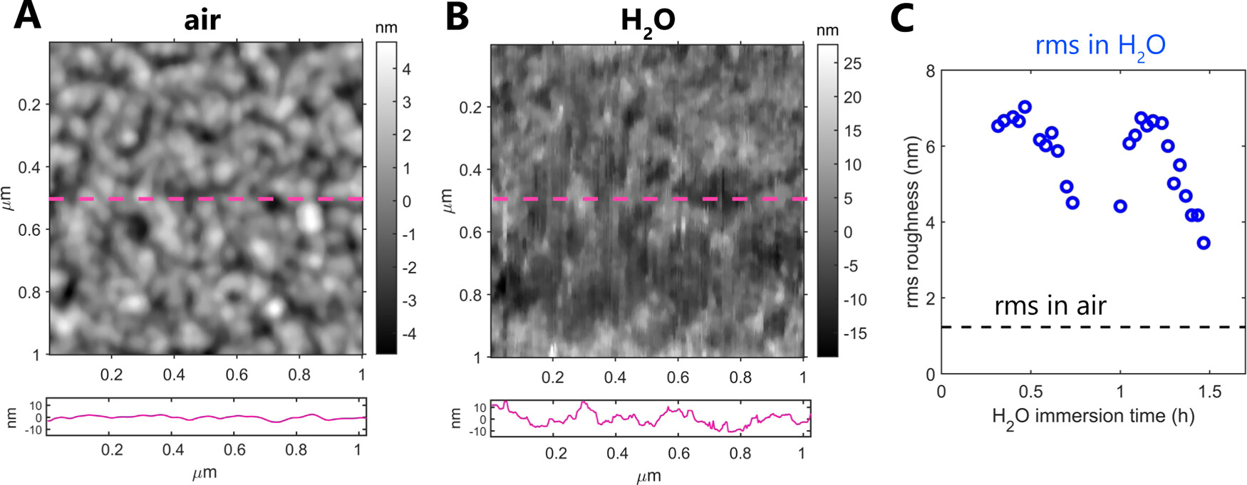
Figure 6. Atomic force microscopy topography maps of calcium silicate films in air (A) and in water ((B) sample immersed in H2O for 30 min). The panels below AFM maps show height profiles along the center of each AFM image as marked with a dashed magenta line. Note that the y axis is the same in both panels. (C) Comparison of the root-mean-square (rms) roughness measured in air and in water (over 1.5 h in the same position) for a 1 × 1 μm2 scan size. Each point corresponds to one AFM scan, including the measurement in air. NanoWorld ARROW-UHFAuD AFM probes were used.
Figure 6 from “Detecting Early-Stage Cohesion Due to Calcium Silicate Hydration with Rheology and Surface Force Apparatus “ by Teresa Liberto et al.:
Atomic force microscopy topography maps of calcium silicate films in air (A) and in water ((B) sample immersed in H2O for 30 min). The panels below AFM maps show height profiles along the center of each AFM image as marked with a dashed magenta line. Note that the y axis is the same in both panels. (C) Comparison of the root-mean-square (rms) roughness measured in air and in water (over 1.5 h in the same position) for a 1 × 1 μm2 scan size. Each point corresponds to one AFM scan, including the measurement in air.

*Teresa Liberto, Andreas Nenning, Maurizio Bellotto, Maria Chiara Dalconi, Dominik Dworschak, Lukas Kalchgruber, Agathe Robisson, Markus Valtiner and Joanna Dziadkowiec
Detecting Early-Stage Cohesion Due to Calcium Silicate Hydration with Rheology and Surface Force Apparatus
Langmuir 2022, 38, 48, 14988–15000
DOI: https://doi.org/10.1021/acs.langmuir.2c02783

The article “Detecting Early-Stage Cohesion Due to Calcium Silicate Hydration with Rheology and Surface Force Apparatus” by Teresa Liberto, Andreas Nenning, Maurizio Bellotto, Maria Chiara Dalconi, Dominik Dworschak, Lukas Kalchgruber, Agathe Robisson, Markus Valtiner and Joanna Dziadkowiec is licensed under a Creative Commons Attribution 4.0 International License, which permits use, sharing, adaptation, distribution and reproduction in any medium or format, as long as you give appropriate credit to the original author(s) and the source, provide a link to the Creative Commons license, and indicate if changes were made. The images or other third-party material in this article are included in the article’s Creative Commons license, unless indicated otherwise in a credit line to the material. If material is not included in the article’s Creative Commons license and your intended use is not permitted by statutory regulation or exceeds the permitted use, you will need to obtain permission directly from the copyright holder. To view a copy of this license, visit https://creativecommons.org/licenses/by/4.0/.

Feasibility of wear reduction for soft nanostructured thin film through enhanced elastic recoverability and contact stress relief

Over several decades many studies on the reduction of wear of mechanical systems have been conducted.
Methods to reduce wear are generally divided into the following categories: applying lubrication, coating with high-hardness materials, and surface texturing. *

Several studies have reported that coatings with higher hardness show more wear than those with lower hardness. From these reports, it is apparent that wear does not depend solely on the hardness of the surface.  Hence, there is a strong motivation for utilizing additional strategies for designing wear-resistive surfaces rather than only enhancing the hardness of the coating. *

In the article “Feasibility of wear reduction for soft nanostructured thin film through enhanced elastic recoverability and contact stress relief” Kuk-Jin Seo, Hyun-Joon Kim and Dae-Eun Kim show, that a soft, thin film comprising randomly aligned carbon nanotubes (CNTs) can reduce surface wear more effectively than a homogeneous thin film because of enhanced elastic recoverability and contact stress relief originating from its mesh structure. *

To investigate the wear characteristics of the mesh structure compared to those of the homogeneous thin film, multi-walled CNTs (MWCNTs) and diamond-like carbon (DLC) thin films were prepared to conduct nanoscale tribological experiments using atomic force microscopy (AFM). The MWCNT thin film showed unmeasurably low wear compared with the DLC thin film under a certain range of normal load. *

To demonstrate the wear reduction mechanism of the MWCNT thin film, its indentation and frictional behaviors were assessed. The indentation behavior of the MWCNT thin film revealed repetitive elastic deformation with a wide strain range and a significantly lower elastic modulus than that of the DLC thin film. The permanent deformation of the MWCNT thin film was observed through frictional experiments under relatively high normal load conditions. *

The presented results are expected to provide insights into the design of highly wear-resistant surfaces using nanostructures. *

The thickness and surface roughness of the MWCNT and DL thin films were measured using Atomic Force Microscopy. *

The force-displacement (F-D) curves were measured on the MWCNT thin film using the AFM to verify the mechanical behavior when indented by the zirconia microspheres that were used for wear and friction experiments. *

The adhesion forces between the thin films and zirconia microspheres were measured by observing the pull-off force of the F-D curve with the AFM. *

The adhesion force was measured using a colloidal AFM probe to aid the analysis of the tribological characteristics of the thin film. *

The pull-off forces for the DL specimens were obtained at 35 different locations with displacements of 50-200 nm. *

Diamond-coated AFM probes (NanoWorld Pointprobe® DT-NCHR ) were used for scanning, while non-coated silicon AFM probes with relatively high and low spring constants (NanoWorld Pointprobe® NCHR and CONTR) were used for the tribological experiments and specimen characterizations. *

Diamond-coated AFM probes (NanoWorld Pointprobe® DT-NCHR ) were used for scanning, while non-coated silicon AFM probes with relatively high and low spring constants (NanoWorld Pointprobe® NCHR and CONTR) were used for the tribological experiments and specimen characterizations.
Figure 6 from “Feasibility of wear reduction for soft nanostructured thin film through enhanced elastic recoverability and contact stress relief” by Kuk-Jin Seo et al.:
AFM images of wear tracks on the MWCNT thin film under test conditions of (a) 2,000 nN and 20,000 cycles, (b) 6,000 nN and 30,000 cycles, (c) 7,000 nN and 30,000 cycles, (d) 9,200 nN and 30,000 cycles, (e) 13,500 nN and 30,000 cycles, and (f) 28,000 nN and 30,000 cycles. Post-processed AFM images that subtracted the original image before each wear test under conditions of (g) 6,000 nN and 30,000 cycles, (h) 7,000 nN and 30,000 cycles, and (i) 28,000 nN and 30,000 cycles

*Kuk-Jin Seo, Hyun-Joon Kim and Dae-Eun Kim
Feasibility of wear reduction for soft nanostructured thin film through enhanced elastic recoverability and contact stress relief
Friction 11(7): 1292-1306 (2023)
DOI: https://doi.org/10.1007/s40544-022-0669-7

Please follow this external link to read the full article: https://rdcu.be/dejTa

The article “Feasibility of wear reduction for soft nanostructured thin film through enhanced elastic recoverability and contact stress relief” by Kuk-Jin Seo, Hyun-Joon Kim and Dae-Eun Kim is licensed under a Creative Commons Attribution 4.0 International License, which permits use, sharing, adaptation, distribution and reproduction in any medium or format, as long as you give appropriate credit to the original author(s) and the source, provide a link to the Creative Commons license, and indicate if changes were made. The images or other third-party material in this article are included in the article’s Creative Commons license, unless indicated otherwise in a credit line to the material. If material is not included in the article’s Creative Commons license and your intended use is not permitted by statutory regulation or exceeds the permitted use, you will need to obtain permission directly from the copyright holder. To view a copy of this license, visit https://creativecommons.org/licenses/by/4.0/.

Impact of annealing on electric and elastic properties of 10-nm Hf0.5Zr0.5O2 films prepared on Si by sputtering

HfO2-based films are important materials used in broad range of electronic applications from high-performance transistors and memory cells, to thermoelectric and energy harvesting elements. *

In the article “Impact of annealing on electric and elastic properties of 10-nm Hf0.5Zr0.5O2 films prepared on Si by sputtering” Leonid Bolotov, Shinji Migita, Ryouta Fujio, Manabu Ishimaru, Shogo Hatayama and Noriyuki Uchida described how they used scanning probe methods to make nanoscale comparison of chemical composition, surface morphology, the elastic modulus and the surface potential of bare 10-nm thick Hf0.5Zr0.5O2 films prepared on Si by a carbon-free sputtering process. *

NanoWorld conductive platinum iridium5 coated Pointprobe® EFM AFM probes were used for the electrostatic force microscopy (EFM). *

The composition mapping confirmed uniform distribution of Hf and Zr in the film along wafer size. Suppression of the monoclinic phase in films annealed at 600 – 800 °C had strong impact on spatial variations of film properties. Small surface roughness, large electric domain sizes (50–200 nm at 700 °C) and small fluctuations of the surface potential (40–50 meV) in Si coated with the films are appealing for gate-stack applications. Films annealed at 600-700 °C showed the elastic modulus of about 169 GPa and the ferroelectric polarization reversal at a field of ~1 MV/cm as observed by nanoscale poling with a Pt-coated scanning probe. In contrast, properties of films annealing at 800 °C were affected by growth of thick interfacial oxide layer. *

The nanoscale approach presented in the article is beneficial in optimizing of physical and mechanical properties of thin dielectric films. *

Fig. 3 from Leonid Bolotov et al. “Impact of annealing on electric and elastic properties of 10-nm Hf0.5Zr0.5O2 films prepared on Si by sputtering”: AFM topographs (a, c) and CPD maps (b, d) of 10 nm Hf0.5Zr0.5O2 films on Si: as-grown film (a, b), and annealed at 700 °C (c, d). Rectangular shapes in (c, d) outline one domain. Scale bars are 200 nm. NanoWorld conductive platinum iridium5 coated Pointprobe® EFM AFM probes were used for the electrostatic force microscopy (EFM).
Fig. 3 from Leonid Bolotov et al. “Impact of annealing on electric and elastic properties of 10-nm Hf0.5Zr0.5O2 films prepared on Si by sputtering”:
AFM topographs (a, c) and CPD maps (b, d) of 10 nm Hf0.5Zr0.5O2 films on Si: as-grown film (a, b), and annealed at 700 °C (c, d). Rectangular shapes in (c, d) outline one domain. Scale bars are 200 nm.

*Leonid Bolotov, Shinji Migita, Ryouta Fujio, Manabu Ishimaru, Shogo Hatayama and Noriyuki Uchida
Impact of annealing on electric and elastic properties of 10-nm Hf0.5Zr0.5O2 films prepared on Si by sputtering
Microelectronic Engineering, Volume 258, 1 April 2022, 111770
DOI: https://doi.org/10.1016/j.mee.2022.111770

Open Access The article “Impact of annealing on electric and elastic properties of 10-nm Hf0.5Zr0.5O2 films prepared on Si by sputtering” by Leonid Bolotov, Shinji Migita, Ryouta Fujio, Manabu Ishimaru, Shogo Hatayama and Noriyuki Uchida is licensed under a Creative Commons Attribution 4.0 International License, which permits use, sharing, adaptation, distribution and reproduction in any medium or format, as long as you give appropriate credit to the original author(s) and the source, provide a link to the Creative Commons license, and indicate if changes were made. The images or other third party material in this article are included in the article’s Creative Commons license, unless indicated otherwise in a credit line to the material. If material is not included in the article’s Creative Commons license and your intended use is not permitted by statutory regulation or exceeds the permitted use, you will need to obtain permission directly from the copyright holder. To view a copy of this license, visit http://creativecommons.org/licenses/by/4.0/.