NanoWorld AG CEO Manfred Detterbeck will be at the NanoAndMore Japan booth at the 63rd Annual Meeting of the Biophysical Society of Japan held from September 24– 26, 2025 at Nara Prefectural Convention Center. Will we meet you there too?
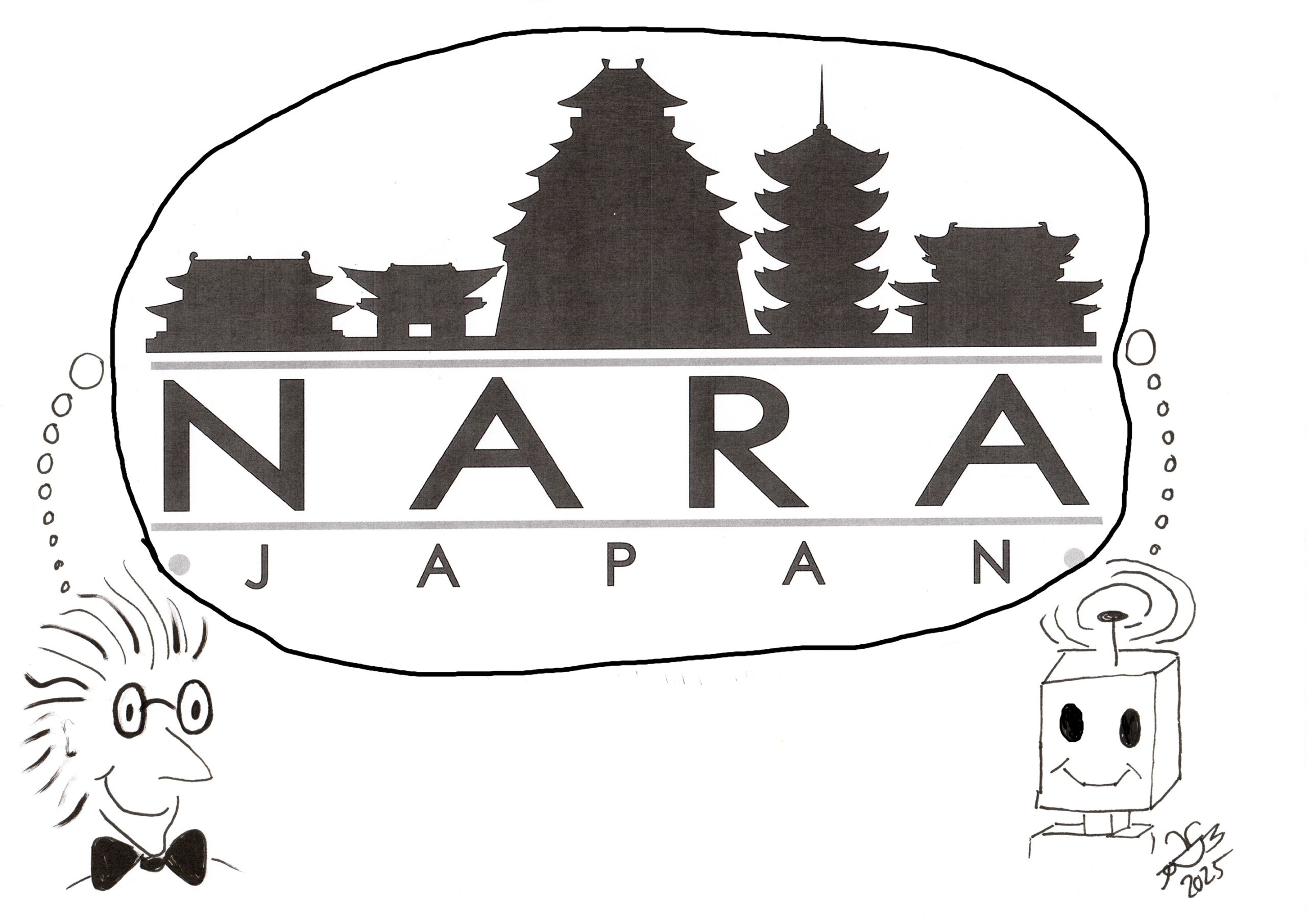
Skyline of Nara
JosepPerianes/Shutterstock.com