Active self-assembly of piezoelectric biomolecular films via synergistic nanoconfinement and in-situ poling

Piezoelectric biomaterials have attracted great attention owing to the recent recognition of the impact of piezoelectricity on biological systems and their potential applications in implantable sensors, actuators, and energy harvesters. However, their practical use is hindered by the weak piezoelectric effect caused by the random polarization of biomaterials and the challenges of large-scale alignment of domains.*

In the article “Active self-assembly of piezoelectric biomolecular films via synergistic nanoconfinement and in-situ poling” Zhuomin Zhang, Xuemu Li, Zehua Peng, Xiaodong Yan, Shiyuan Liu, Ying Hong, Yao Shan, Xiaote Xu, Lihan Jin, Bingren Liu, Xinyu Zhang, Yu Chai, Shujun Zhang, Alex K.-Y. Jen and Zhengbao Yang present an active self-assembly strategy to tailor piezoelectric biomaterial thin films.*

The nanoconfinement-induced homogeneous nucleation overcomes the interfacial dependency and allows the electric field applied in-situ to align crystal grains across the entire film. The β-glycine films exhibit an enhanced piezoelectric strain coefficient of 11.2 pm V−1 and an exceptional piezoelectric voltage coefficient of 252 × 10−3 Vm N−1. Of particular significance is that the nanoconfinement effect greatly improves the thermostability before melting (192 °C). *

This finding offers a generally applicable strategy for constructing high-performance large-sized piezoelectric bio-organic materials for biological and medical microdevices.*

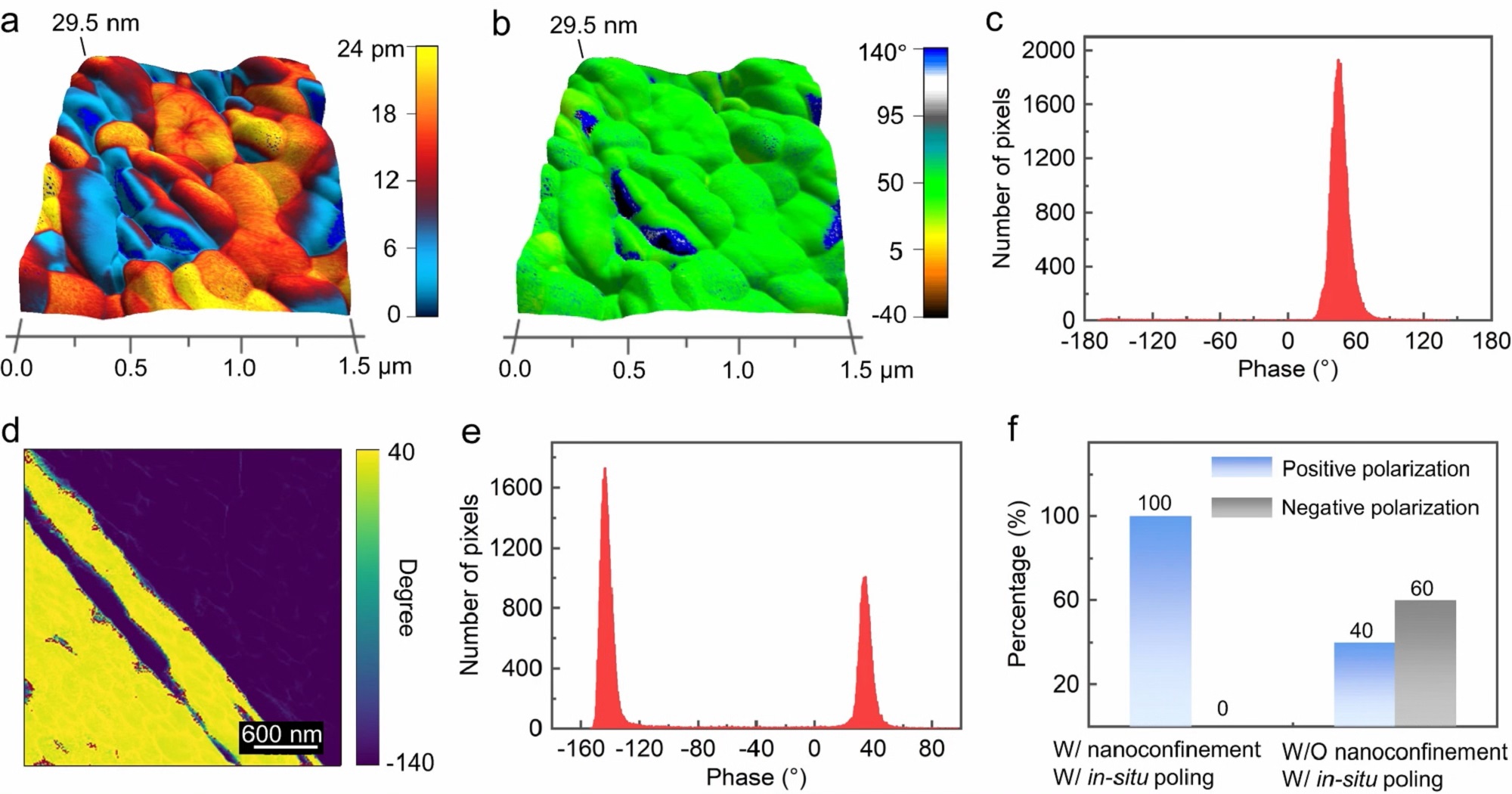
The piezoelectric properties of the as-prepared β-glycine nanocrystalline films were evaluated by piezoresponse force microscopy (PFM) measurements.*

For all piezoresponse force microscopy (PFM) measurements and SKPM (scanning Kelvin probe force microscopy) measurements mentioned in this article, conductive NanoWorld Arrow-EFM AFM probes with PtIr coating on both AFM cantilever and AFM tip were used. The nominal resonance frequency and the nominal stiffness of the AFM probe are 75 kHz and 2.8 N m−1, respectively.

Figure 3 from “Active self-assembly of piezoelectric biomolecular films via synergistic nanoconfinement and in-situ poling” by Zhuomin Zhang et al.:PFM measurements and polarization alignment studies of β-glycine nanocrystalline films. a The PFM OOP amplitude mapping overlaid on the 3D topography of as-prepared films in a 1.5 × 1.5 µm2 area. The applied AC voltage is 2 V. b The corresponding PFM OOP phase mapping overlaid on the 3D topography. c Histogram calculated from the PFM OOP phase mapping in (b) showing that the β-glycine nanocrystalline films are dominated by domains with the unique polarization direction. d PFM OOP phase mapping of the β-glycine microcrystals obtained by electrohydrodynamic focusing deposition through heterogeneous nucleation. e Histogram calculated from the phase mapping in (d). f Comparison of statistics of the piezoelectric phase for the as-prepared β-glycine nanocrystalline films via synergistic nanoconfinement and in-situ poling (left), and β-glycine microcrystals grown by heterogeneous nucleation in the absence of nanoconfinement effect (right). NanoWorld conductive Arrow-EFM AFM probes were used for the piezoresponse force microscopy (PFM) and scanning Kelvin probe force microscopy (SKPFM) measurements mentioned in this article.
Figure 3 from “Active self-assembly of piezoelectric biomolecular films via synergistic nanoconfinement and in-situ poling” by Zhuomin Zhang et al.:
PFM measurements and polarization alignment studies of β-glycine nanocrystalline films.
a The PFM OOP amplitude mapping overlaid on the 3D topography of as-prepared films in a 1.5 × 1.5 µm2 area. The applied AC voltage is 2 V. b The corresponding PFM OOP phase mapping overlaid on the 3D topography. c Histogram calculated from the PFM OOP phase mapping in (b) showing that the β-glycine nanocrystalline films are dominated by domains with the unique polarization direction. d PFM OOP phase mapping of the β-glycine microcrystals obtained by electrohydrodynamic focusing deposition through heterogeneous nucleation. e Histogram calculated from the phase mapping in (d). f Comparison of statistics of the piezoelectric phase for the as-prepared β-glycine nanocrystalline films via synergistic nanoconfinement and in-situ poling (left), and β-glycine microcrystals grown by heterogeneous nucleation in the absence of nanoconfinement effect (right).

*Zhuomin Zhang, Xuemu Li, Zehua Peng, Xiaodong Yan, Shiyuan Liu, Ying Hong, Yao Shan, Xiaote Xu, Lihan Jin, Bingren Liu, Xinyu Zhang, Yu Chai, Shujun Zhang, Alex K.-Y. Jen and Zhengbao Yang
Active self-assembly of piezoelectric biomolecular films via synergistic nanoconfinement and in-situ poling
Nature Communications volume 14, Article number: 4094 (2023)
DOI: https://doi.org/10.1038/s41467-023-39692-y

Please follow this external link to read the full article: https://rdcu.be/dzddh

The article “Active self-assembly of piezoelectric biomolecular films via synergistic nanoconfinement and in-situ poling” by Zhuomin Zhang, Xuemu Li, Zehua Peng, Xiaodong Yan, Shiyuan Liu, Ying Hong, Yao Shan, Xiaote Xu, Lihan Jin, Bingren Liu, Xinyu Zhang, Yu Chai, Shujun Zhang, Alex K.-Y. Jen and Zhengbao Yang is licensed under a Creative Commons Attribution 4.0 International License, which permits use, sharing, adaptation, distribution and reproduction in any medium or format, as long as you give appropriate credit to the original author(s) and the source, provide a link to the Creative Commons license, and indicate if changes were made. The images or other third-party material in this article are included in the article’s Creative Commons license, unless indicated otherwise in a credit line to the material. If material is not included in the article’s Creative Commons license and your intended use is not permitted by statutory regulation or exceeds the permitted use, you will need to obtain permission directly from the copyright holder. To view a copy of this license, visit https://creativecommons.org/licenses/by/4.0/.

Cross-sectional Kelvin probe force microscopy on III–V epitaxial multilayer stacks: challenges and perspectives

The development of photovoltaic (PV) technologies has progressed significantly over the past twenty years as a result of considerable advancements in solar cell device engineering and material science. *

As a consequence, solar cells have turned into complex structures containing numerous layers and interfaces. The capability to conduct local investigations at the nanoscale level that provide information on the electrical properties of materials and along physical interfaces is becoming crucial for solar photovoltaic device efficiency improvement. *

The capability to conduct local investigations at the nanoscale level that provide information on the electrical properties of materials and along physical interfaces is becoming crucial for solar photovoltaic device efficiency improvement. *

Multilayer III–V-based solar cells are complex devices consisting of many layers and interfaces. *

The study and the comprehension of the mechanisms that take place at the interfaces is crucial for efficiency improvement. *

Electrical measurements based on scanning probe microscopy (SPM) allow for the analysis of two-dimensional (2D) features at the surface and along a physical cross section of nanoscale semiconductor structures. *

Among the wide variety of SPM techniques available, Kelvin probe force microscopy (KPFM) is an application of the atomic force microscope (AFM) for the evaluation of the surface potential with nanometric resolution. KPFM is a valuable investigative approach for the study of work functions via the measurement of the contact potential difference VCPD, that is, the difference between the electrostatic potential at the surface of the investigated structure and that of the KPFM probe. *

In the article “Cross-sectional Kelvin probe force microscopy on III–V epitaxial multilayer stacks: challenges and perspectives” Mattia da Lisca, José Alvarez, James P. Connolly, Nicolas Vaissiere, Karim Mekhazni, Jean Decobert and Jean-Paul Kleider apply frequency-modulated Kelvin probe force microscopy (FM-KPFM) under ambient conditions to investigate the capability of this technique for the analysis of an InP/GaInAs(P) multilayer stack. *

KPFM reveals a strong dependence on the local doping concentration, allowing for the detection of the surface potential of layers with a resolution as low as 20 nm. *

The analysis of the surface potential allowed for the identification of space charge regions and, thus, the presence of several junctions along the stack. Furthermore, a contrast enhancement in the surface potential image was observed when KPFM was performed under illumination, which is analysed in terms of the reduction of surface band bending induced by surface defects by photogenerated carrier distributions. The analysis of the KPFM data was assisted by means of theoretical modelling simulating the energy bands profile and KPFM measurements. *

KPFM was performed using a scanning probe microscopy system under ambient conditions and operated in the frequency-modulated KPFM (FM-KPFM) mode using a two-pass scanning mode, where the second pass was performed at a constant distance of 10 nm from the sample surface. *

The FM-KPFM mode was chosen over the amplitude-modulation mode (AM-KPFM) since it is well known that it provides better spatial resolution. In particular, in AM-KPFM the electrical force between the tip and the sample is directly evaluated, whereas in FM-KPFM the gradient of the force is analysed. As a result, FM-KPFM is more sensitive to local tip apex–sample surface interactions; therefore, long-range electrostatic interactions of the cantilever are reduced, as well as the effect of parasitic capacitances. Additionally, in FM-KPFM, surface potential measurements are less dependent on the lift-height tip–sample distance than in AM-KPFM since this mode is less sensitive to static offsets induced by capacitive coupling or crosstalk. *

The laser beam deflection system in the author’s AFM employs a laser wavelength of 1310 nm, which is well below the bandgap of the sample; therefore, the parasitic laser absorption, which may interfere with the KPFM measurement, is reduced to negligible levels. Highly doped NanoWorld n+-Si ARROW-EFM tips (typical AFM tip radius < 25 nm) with a conductive Pt/Ir coating at a typical resonance frequency of 75 kHz were used. *

Figure 4 from “Cross-sectional Kelvin probe force microscopy on III–V epitaxial multilayer stacks: challenges and perspectives” by Mattia da Lisca et al : KPFM measurement under ambient conditions on the surface cross section of the sample under illumination: (a) topography and (b) VCPD image. A vertical coloured bar is included to ease the identification of the different layers. The profile in (c) corresponds to the region identified by the dotted white segments in (b), each point of the profile (vertical) direction being an average of 207 points over a width of 0.7 μm along the x axis. Several regions along the structure have been highlighted using different colours (see text). The black arrow indicates the space charge region at the InP:nid/InP:Zn interface. Highly doped NanoWorld n+-Si ARROW-EFM AFM probes (typical AFM tip radius < 25 nm) with a conductive Pt/Ir coating at a typical resonance frequency of 75 kHz were used.
Figure 4 from “Cross-sectional Kelvin probe force microscopy on III–V epitaxial multilayer stacks: challenges and perspectives” by Mattia da Lisca et al :
KPFM measurement under ambient conditions on the surface cross section of the sample under illumination: (a) topography and (b) VCPD image. A vertical coloured bar is included to ease the identification of the different layers. The profile in (c) corresponds to the region identified by the dotted white segments in (b), each point of the profile (vertical) direction being an average of 207 points over a width of 0.7 μm along the x axis. Several regions along the structure have been highlighted using different colours (see text). The black arrow indicates the space charge region at the InP:nid/InP:Zn interface.

*Mattia da Lisca, José Alvarez, James P. Connolly, Nicolas Vaissiere, Karim Mekhazni, Jean Decobert and  Jean-Paul Kleider
Cross-sectional Kelvin probe force microscopy on III–V epitaxial multilayer stacks: challenges and perspectives
Beilstein Journal of Nanotechnology 2023, 14, 725–737
DOI: https://doi.org/10.3762/bjnano.14.59

The article “Cross-sectional Kelvin probe force microscopy on III–V epitaxial multilayer stacks: challenges and perspectives” by Mattia da Lisca, José Alvarez, James P. Connolly, Nicolas Vaissiere, Karim Mekhazni, Jean Decobert and  Jean-Paul Kleider is licensed under a Creative Commons Attribution 4.0 International License, which permits use, sharing, adaptation, distribution and reproduction in any medium or format, as long as you give appropriate credit to the original author(s) and the source, provide a link to the Creative Commons license, and indicate if changes were made. The images or other third-party material in this article are included in the article’s Creative Commons license, unless indicated otherwise in a credit line to the material. If material is not included in the article’s Creative Commons license and your intended use is not permitted by statutory regulation or exceeds the permitted use, you will need to obtain permission directly from the copyright holder. To view a copy of this license, visit https://creativecommons.org/licenses/by/4.0/.
Influence of B/N co-doping on electrical and photoluminescence properties of CVD grown homoepitaxial diamond films

Boron doped diamond (BDD) has great potential in electrical, and electrochemical sensing applications. The growth parameters, substrates, and synthesis method play a vital role in the preparation of semiconducting BDD to metallic BDD. Doping of other elements along with boron (B) into diamond demonstrated improved efficacy of B doping and exceptional properties.*

In the article “Influence of B/N co-doping on electrical and photoluminescence properties of CVD grown homoepitaxial diamond films” Srinivasu Kunuku, Mateusz Ficek, Aleksandra Wieloszynska, Magdalena Tamulewicz-Szwajkowska, Krzysztof Gajewski, Miroslaw Sawczak, Aneta Lewkowicz, Jacek Ryl, Tedor Gotszalk and Robert Bogdanowicz describe how B and nitrogen (N) co-doped diamond has been synthesized on single crystalline diamond (SCD) IIa and SCD Ib substrates in a microwave plasma-assisted chemical vapor deposition process.*

The surface topography of the CVD diamond layers was investigated using atomic force microscopy (AFM), and Kelvin probe force microscopy (KPFM) was employed to measure the contact potential difference (CPD) to calculate the work function of these CVD diamond layers.*

Atomic force microscopy topography depicted the flat and smooth surface with low surface roughness for low B doping, whereas surface features like hillock structures and un-epitaxial diamond crystals with high surface roughness were observed for high B doping concentrations. KPFM measurements revealed that the work function (4.74–4.94 eV) has not varied significantly for CVD diamond synthesized with different B/C concentrations.*

NanoWorld ARROW-EFM conductive platinumirdidium5 coated AFM probes with a typical spring constant of 2.8 N/m and a typical resonant frequency of 75 kHz were used.*

Figure 2 from “Influence of B/N co-doping on electrical and photoluminescence properties of CVD grown homoepitaxial diamond films “ by Srinivasu Kunuku et al: AFM topography of B/N co-doped CVD diamond on (with fixed N/C = 0.02) SCD IIa; (a) B/C ∼ 2500 ppm (b) B/C ∼ 5000 ppm (c) B/C ∼ 7500 ppm, and KPFM CPD images of B/N co-doped CVD diamond (with fixed N/C = 0.02) on SCD IIa; (d) B/C ∼ 2500 ppm (e) B/C ∼ 5000 ppm (f) B/C ∼ 7500 ppm. NanoWorld Arrow-EFM platinumiridium coated AFM probes were used for the KPFM and surface topography measurements.
Figure 2 from “Influence of B/N co-doping on electrical and photoluminescence properties of CVD grown homoepitaxial diamond films “ by Srinivasu Kunuku et al:
AFM topography of B/N co-doped CVD diamond on (with fixed N/C = 0.02) SCD IIa; (a) B/C ∼ 2500 ppm (b) B/C ∼ 5000 ppm (c) B/C ∼ 7500 ppm, and KPFM CPD images of B/N co-doped CVD diamond (with fixed N/C = 0.02) on SCD IIa; (d) B/C ∼ 2500 ppm (e) B/C ∼ 5000 ppm (f) B/C ∼ 7500 ppm.

*Srinivasu Kunuku, Mateusz Ficek, Aleksandra Wieloszynska, Magdalena Tamulewicz-Szwajkowska, Krzysztof Gajewski, Miroslaw Sawczak, Aneta Lewkowicz, Jacek Ryl, Tedor Gotszalk and Robert Bogdanowicz
Influence of B/N co-doping on electrical and photoluminescence properties of CVD grown homoepitaxial diamond films
Nanotechnology (2022),  33 125603
DOI: https://doi.org/10.1088/1361-6528/ac4130

Please follow this external link to read the full article: https://doi.org/10.1088/1361-6528/ac4130

Open Access The article “Influence of B/N co-doping on electrical and photoluminescence properties of CVD grown homoepitaxial diamond films” by Srinivasu Kunuku, Mateusz Ficek, Aleksandra Wieloszynska, Magdalena Tamulewicz-Szwajkowska, Krzysztof Gajewski, Miroslaw Sawczak, Aneta Lewkowicz, Jacek Ryl, Tedor Gotszalk and Robert Bogdanowicz is licensed under a Creative Commons Attribution 4.0 International License, which permits use, sharing, adaptation, distribution and reproduction in any medium or format, as long as you give appropriate credit to the original author(s) and the source, provide a link to the Creative Commons license, and indicate if changes were made. The images or other third party material in this article are included in the article’s Creative Commons license, unless indicated otherwise in a credit line to the material. If material is not included in the article’s Creative Commons license and your intended use is not permitted by statutory regulation or exceeds the permitted use, you will need to obtain permission directly from the copyright holder. To view a copy of this license, visit http://creativecommons.org/licenses/by/4.0/.