Kelvin Probe Force Microscopy (KPFM) has become an essential atomic force microscopy (AFM) technique for investigating surface potentials and charge distributions in electronic and optoelectronic materials. However, conventional KPFM measurements can be affected by thermal drift, probe degradation, and environmental changes during data acquisition, making the accurate characterization of dynamic systems particularly challenging. In this article, Zeinab Eftekhari, Ariane Ufer, Ursula Wurstbauer, and Rebecca Saive introduce synchronized modulation Kelvin probe force microscopy (SM-KPFM), an advanced in-operando approach designed to overcome these limitations.
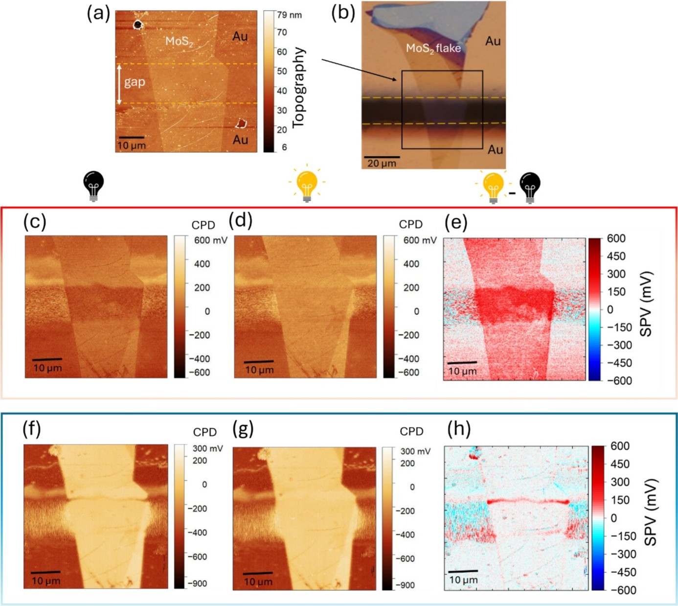
The authors developed SM-KPFM by synchronizing external stimulus modulation, such as illumination or electrical bias, with the AFM scan direction. In synchronized illumination KPFM, the sample remains unilluminated during the trace scan and illuminated during the retrace scan, enabling direct comparison of surface potential states within the same raster image. This strategy minimizes measurement artifacts arising from drift, thermal effects, and AFM probe degradation while providing highly reproducible surface photovoltage measurements.
The technique was demonstrated on a silicon photodiode and a molybdenum disulfide (MoS₂) bilayer deposited on a gold substrate. By capturing illuminated and non-illuminated contact potential difference (CPD) measurements along identical scan paths, SM-KPFM produced accurate, drift-free surface photovoltage maps and provided improved insight into nanoscale photovoltaic behavior and charge separation processes in optoelectronic materials.
Kelvin Probe Force Microscopy measurements were performed in sideband mode using a NanoWorld ARROW-EFM AFM probe. The Pt/Ir-coated AFM probe, featuring a resonance frequency of 68 kHz and a spring constant of 2.8 N/m, enabled highly sensitive surface potential mapping with excellent electrical conductivity and measurement stability. The synchronization approach required only triggering the illumination source using the AFM scan direction signal, making the technique readily applicable to existing KPFM workflows without complex hardware modifications.
This work demonstrates how combining an innovative synchronized measurement strategy with a NanoWorld ARROW-EFM AFM probe significantly improves the reliability of operando Kelvin Probe Force Microscopy. The methodology opens new opportunities for investigating nanoscale electronic and optoelectronic devices, photovoltaic materials, and other functional nanostructures where precise surface potential mapping is essential.
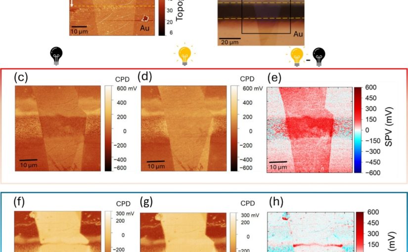
KPFM measurements of a MoS₂ flake on gold electrodes under dark and illuminated conditions. (a) Topography and (b) optical image of the MoS₂ flake on the gold electrodes, where the black box shows the scanned area under AFM/KPFM. The topography image was post-processed to have the substrate and gold contact surfaces on the same level such that the thin flake becomes visible. (c, d) CPD maps acquired in separate scans under dark (c) and illuminated (d) conditions using conventional KPFM (red box). (e) SPV map derived from the sequential scans. (f) Trace (dark) and (g) retrace (illuminated) CPD maps obtained using SM- KPFM (blue box). (h) SPV map (retraced minus trace).
Full citation:
Eftekhari, Z.; Ufer, A.; Wurstbauer, U.; Saive, R. Synchronized modulation Kelvin probe force microscopy for surface photovoltage studies in optoelectronic systems. MRS Communications16 (2026), 180–186. https://doi.org/10.1557/s43579-025-00899-3
Physical properties of the polycrystalline materials are mostly determined by their microstructure. As the crystallization process can determine the microstructure, the nucleation, and growth can also control whether the materials will be resulted in single crystalline or polycrystalline. Along with the morphological changes, anisotropic properties of the materials can also be controlled. *
As a result, preferential orientation with advanced optoelectronic properties can enhance the photovoltaic devices’ performance. *
Although incorporation of additives is one of the most studied methods to stabilize the photoactive α-phase of formamidinium lead tri-iodide (α-FAPbI3), no studies focus on how the additives affect the crystallization kinetics. *
In the article “Kinetic-Controlled Crystallization of α-FAPbI3 Inducing Preferred Crystallographic Orientation Enhances Photovoltaic Performance” along with the role of methylammonium chloride (MACl) as a “stabilizer” in the formation of α-FAPbI3, Sooeun Shin, Seongrok Seo, Seonghwa Jeong, Anir S. Sharbirin, Jeongyong Kim, Hyungju Ahn, Nam-Gyu Park and Hyunjung Shin point out the additional role as a “controller” in the crystallization kinetics. *
With microscopic observations, for example, electron backscatter diffraction and selected area electron diffraction, it is examined that higher concentration of MACl induces slower crystallization kinetics, resulting in larger grain size and [100] preferred orientation. *
Optoelectronic properties of [100] preferentially oriented grains with less non-radiative recombination, a longer lifetime of charge carriers, and lower photocurrent deviations in between each grain induce higher short-circuit current density (Jsc) and fill factor. *
Resulting MACl40 mol% attains the highest power conversion efficiency (PCE) of 24.1%.
The results provide observations of a direct correlation between the crystallographic orientation and device performance as it highlights the importance of crystallization kinetics resulting in desirable microstructures for device engineering. *
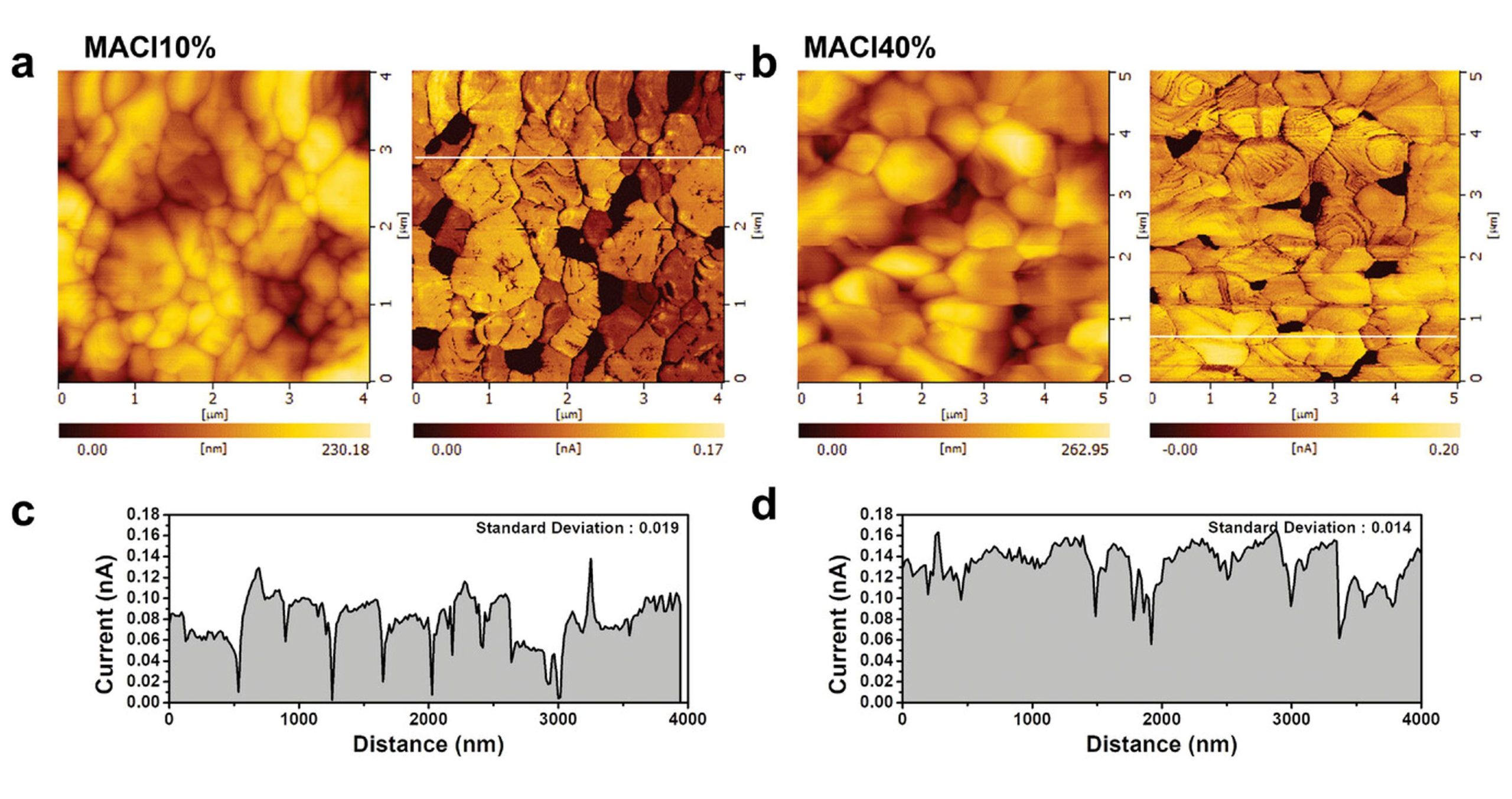
The electrical characterizations with atomic force microscopy (AFM) and conductive atomic force microscopy ( C-AFM) were done to measure the local conductance of FAPbI3 films. All measurements were performed under illumination (green LED) with a 1.3 V bias using a Pt-coated C-AFM probe (NanoWorld PlatinumIridium coated Pointprobe®CONTPt ). FTO was used for the conductive substrates. *
Conductive atomic force microscopy (C-AFM) indicated much more homogeneous photocurrent generation along the surface of (100) preferentially oriented layers. *
Figure 4 from Sooeun Shin et al. 2023 “Kinetic-Controlled Crystallization of α-FAPbI3 Inducing Preferred Crystallographic Orientation Enhances Photovoltaic Performance”: Electrical properties of (100)-oriented α-FAPbI3 thin films. a,b) Surface topography and photocurrent measurement by C-AFM of MACl10% and MACl40%. Measurements were taken under illumination (green LED) with a 1.3 V bias. Current images indicate that photocurrents were induced grain by grain, as each grain showed a distinct photocurrent. The photocurrent deviation for each grain is larger in MACl10% than in MACl40%, which shows a similar photocurrent grain by grain. c,d) Current line profile extracted from the current image (a and b). The standard deviation calculated from the magnitude of the photocurrent in each grain is displayed in the inset (0.019 and 0.014 nA for MACl10% and MACl40%, respectively). A low photocurrent was exhibited at the grain boundaries in both MACl10% and MACl40%. The dark areas measured within the current images are most likely distributed between grain edges. This may be caused by the formation of PbI2 or the loss of contact between the grain and the conducting substrate.
*Sooeun Shin, Seongrok Seo, Seonghwa Jeong, Anir S. Sharbirin, Jeongyong Kim, Hyungju Ahn, Nam-Gyu Park and Hyunjung Shin Kinetic-Controlled Crystallization of α-FAPbI3 Inducing Preferred Crystallographic Orientation Enhances Photovoltaic Performance
Advanced Science, Volume 10, Issue 14, May 17, 2023, 2300798
DOI: https://doi.org/10.1002/advs.202300798
Open Access The article “Kinetic-Controlled Crystallization of α-FAPbI3 Inducing Preferred Crystallographic Orientation Enhances Photovoltaic Performance” Sooeun Shin, Seongrok Seo, Seonghwa Jeong, Anir S. Sharbirin, Jeongyong Kim, Hyungju Ahn, Nam-Gyu Park and Hyunjung Shin is licensed under a Creative Commons Attribution 4.0 International License, which permits use, sharing, adaptation, distribution and reproduction in any medium or format, as long as you give appropriate credit to the original author(s) and the source, provide a link to the Creative Commons license, and indicate if changes were made. The images or other third party material in this article are included in the article’s Creative Commons license, unless indicated otherwise in a credit line to the material. If material is not included in the article’s Creative Commons license and your intended use is not permitted by statutory regulation or exceeds the permitted use, you will need to obtain permission directly from the copyright holder. To view a copy of this license, visit http://creativecommons.org/licenses/by/4.0/.
The development of photovoltaic (PV) technologies has progressed significantly over the past twenty years as a result of considerable advancements in solar cell device engineering and material science. *
As a consequence, solar cells have turned into complex structures containing numerous layers and interfaces. The capability to conduct local investigations at the nanoscale level that provide information on the electrical properties of materials and along physical interfaces is becoming crucial for solar photovoltaic device efficiency improvement. *
The capability to conduct local investigations at the nanoscale level that provide information on the electrical properties of materials and along physical interfaces is becoming crucial for solar photovoltaic device efficiency improvement. *
Multilayer III–V-based solar cells are complex devices consisting of many layers and interfaces. *
The study and the comprehension of the mechanisms that take place at the interfaces is crucial for efficiency improvement. *
Electrical measurements based on scanning probe microscopy (SPM) allow for the analysis of two-dimensional (2D) features at the surface and along a physical cross section of nanoscale semiconductor structures. *
Among the wide variety of SPM techniques available, Kelvin probe force microscopy (KPFM) is an application of the atomic force microscope (AFM) for the evaluation of the surface potential with nanometric resolution. KPFM is a valuable investigative approach for the study of work functions via the measurement of the contact potential difference VCPD, that is, the difference between the electrostatic potential at the surface of the investigated structure and that of the KPFM probe. *
In the article “Cross-sectional Kelvin probe force microscopy on III–V epitaxial multilayer stacks: challenges and perspectives” Mattia da Lisca, José Alvarez, James P. Connolly, Nicolas Vaissiere, Karim Mekhazni, Jean Decobert and Jean-Paul Kleider apply frequency-modulated Kelvin probe force microscopy (FM-KPFM) under ambient conditions to investigate the capability of this technique for the analysis of an InP/GaInAs(P) multilayer stack. *
KPFM reveals a strong dependence on the local doping concentration, allowing for the detection of the surface potential of layers with a resolution as low as 20 nm. *
The analysis of the surface potential allowed for the identification of space charge regions and, thus, the presence of several junctions along the stack. Furthermore, a contrast enhancement in the surface potential image was observed when KPFM was performed under illumination, which is analysed in terms of the reduction of surface band bending induced by surface defects by photogenerated carrier distributions. The analysis of the KPFM data was assisted by means of theoretical modelling simulating the energy bands profile and KPFM measurements. *
KPFM was performed using a scanning probe microscopy system under ambient conditions and operated in the frequency-modulated KPFM (FM-KPFM) mode using a two-pass scanning mode, where the second pass was performed at a constant distance of 10 nm from the sample surface. *
The FM-KPFM mode was chosen over the amplitude-modulation mode (AM-KPFM) since it is well known that it provides better spatial resolution. In particular, in AM-KPFM the electrical force between the tip and the sample is directly evaluated, whereas in FM-KPFM the gradient of the force is analysed. As a result, FM-KPFM is more sensitive to local tip apex–sample surface interactions; therefore, long-range electrostatic interactions of the cantilever are reduced, as well as the effect of parasitic capacitances. Additionally, in FM-KPFM, surface potential measurements are less dependent on the lift-height tip–sample distance than in AM-KPFM since this mode is less sensitive to static offsets induced by capacitive coupling or crosstalk. *
The laser beam deflection system in the author’s AFM employs a laser wavelength of 1310 nm, which is well below the bandgap of the sample; therefore, the parasitic laser absorption, which may interfere with the KPFM measurement, is reduced to negligible levels. Highly doped NanoWorld n+-Si ARROW-EFM tips (typical AFM tip radius < 25 nm) with a conductive Pt/Ir coating at a typical resonance frequency of 75 kHz were used. *
Figure 4 from “Cross-sectional Kelvin probe force microscopy on III–V epitaxial multilayer stacks: challenges and perspectives” by Mattia da Lisca et al : KPFM measurement under ambient conditions on the surface cross section of the sample under illumination: (a) topography and (b) VCPD image. A vertical coloured bar is included to ease the identification of the different layers. The profile in (c) corresponds to the region identified by the dotted white segments in (b), each point of the profile (vertical) direction being an average of 207 points over a width of 0.7 μm along the x axis. Several regions along the structure have been highlighted using different colours (see text). The black arrow indicates the space charge region at the InP:nid/InP:Zn interface.
*Mattia da Lisca, José Alvarez, James P. Connolly, Nicolas Vaissiere, Karim Mekhazni, Jean Decobert and Jean-Paul Kleider Cross-sectional Kelvin probe force microscopy on III–V epitaxial multilayer stacks: challenges and perspectives
Beilstein Journal of Nanotechnology 2023, 14, 725–737
DOI: https://doi.org/10.3762/bjnano.14.59
The article “Cross-sectional Kelvin probe force microscopy on III–V epitaxial multilayer stacks: challenges and perspectives” by Mattia da Lisca, José Alvarez, James P. Connolly, Nicolas Vaissiere, Karim Mekhazni, Jean Decobert and Jean-Paul Kleider is licensed under a Creative Commons Attribution 4.0 International License, which permits use, sharing, adaptation, distribution and reproduction in any medium or format, as long as you give appropriate credit to the original author(s) and the source, provide a link to the Creative Commons license, and indicate if changes were made. The images or other third-party material in this article are included in the article’s Creative Commons license, unless indicated otherwise in a credit line to the material. If material is not included in the article’s Creative Commons license and your intended use is not permitted by statutory regulation or exceeds the permitted use, you will need to obtain permission directly from the copyright holder. To view a copy of this license, visit https://creativecommons.org/licenses/by/4.0/.