Quantification of electron accumulation at grain boundaries in perovskite polycrystalline films by correlative infrared-spectroscopic nanoimaging and Kelvin probe force microscopy

Organic-inorganic halide perovskites are materials of high interest for the development of solar cells.

Learning more about the relationship between the electrical properties and the chemical compositions of perovskite at the nanoscale can help to understand how the interrelations of both can affect device performance and contribute to an understanding on how to best design perovskite active layer structures.*

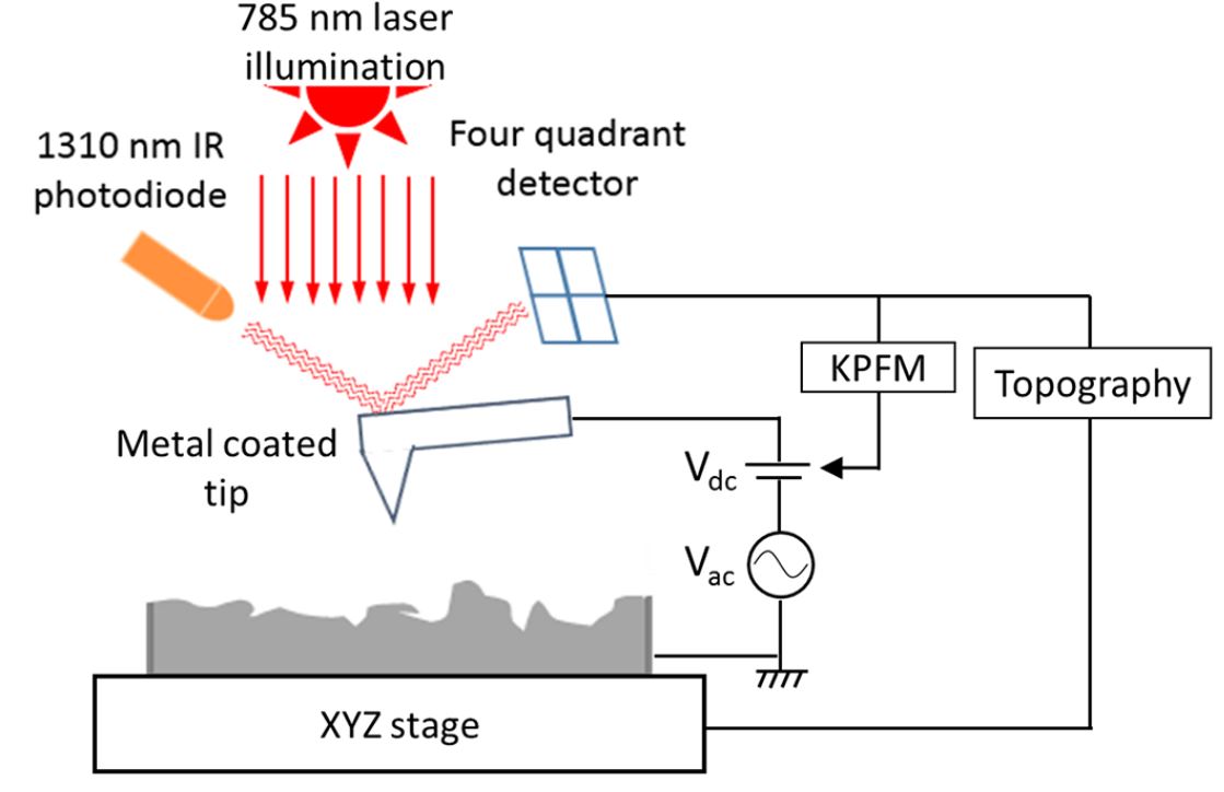
For the article “Quantification of electron accumulation at grain boundaries in perovskite polycrystalline films by correlative infrared-spectroscopic nanoimaging and Kelvin probe force microscopy” Ting-Xiao Qin, En-Ming You, Mao-Xin Zhang, Peng Zheng, Xiao-Feng Huang, Song-Yuan Ding, Bing-Wei Mao and Zhong-Qun Tian used correlative infrared-spectroscopic nanoimaging ( IR-spectroscopy ) by scattering-type scanning near-field optical microscopy ( s-SNOM ) and Kelvin probe force microscopy ( KPFM ) to contribute to the discussion whether nanometer-sized grain boundaries (GBs) in polycrystalline perovskite films play a positive or negative role in solar cell performance.*

The integrated KPFM and s-SNOM measurements were performed by the authors to acquire the surface potential and infrared near-field image simultaneously through a single-pass scan and thereby learn more about the relationships between the electrical properties and spectral information at the grain boundaries of the investigated material ( polycrystalline CH3NH3Pbl3 perovskite films ).*

The results of the correlated s-SNOM and KPFM imaging presented in the article show that the electron accumulations are enhanced at the grain boundaries (GBs) of the investigated polycrystalline perovskite film, particularly under light illumination which would assist in electron-hole separation and therefore would be a positive influence on the performance of the solar cell.*

NanoWorld conductive platinum-iridium coated Arrow AFM probes ( Arrow-NCPt ) were used to perform the s-SNOM IR imaging.

Figure 4 from “Quantification of electron accumulation at grain boundaries in perovskite polycrystalline films by correlative infrared-spectroscopic nanoimaging and Kelvin probe force microscopy” by Ting-Xiao Qin  et al.
Correlative KPFM and s-SNOM nanoimaging on perovskite.
a AFM topography (1 μm × 1 μm); b Contact potential difference (CPD); and c simultaneously acquired infrared near-field image; d one-dimensional line profiles of the topography, CPD and infrared near-field amplitude along the white dashed lines marked in a–c. The scale bars are 200 nm.
NanoWorld Arrow-NCPt AFM probes were used to perform the s-SNOM IR imaging
Figure 4 from “Quantification of electron accumulation at grain boundaries in perovskite polycrystalline films by correlative infrared-spectroscopic nanoimaging and Kelvin probe force microscopy” by Ting-Xiao Qin  et al.
Correlative KPFM and s-SNOM nanoimaging on perovskite.
a AFM topography (1 μm × 1 μm); b Contact potential difference (CPD); and c simultaneously acquired infrared near-field image; d one-dimensional line profiles of the topography, CPD and infrared near-field amplitude along the white dashed lines marked in a–c. The scale bars are 200 nm.

*Ting-Xiao Qin, En-Ming You, Mao-Xin Zhang, Peng Zheng, Xiao-Feng Huang, Song-Yuan Ding, Bing-Wei Mao and Zhong-Qun Tian
Quantification of electron accumulation at grain boundaries in perovskite polycrystalline films by correlative infrared-spectroscopic nanoimaging and Kelvin probe force microscopy
Light: Science & Applications volume 10, Article number: 84 (2021)
DOI: https://doi.org/10.1038/s41377-021-00524-7

Please follow the external link to read the whole article: https://rdcu.be/clg7f

Open Access : The article “Quantification of electron accumulation at grain boundaries in perovskite polycrystalline films by correlative infrared-spectroscopic nanoimaging and Kelvin probe force microscopy” by Ting-Xiao Qin, En-Ming You, Mao-Xin Zhang, Peng Zheng, Xiao-Feng Huang, Song-Yuan Ding, Bing-Wei Mao and Zhong-Qun Tian is licensed under a Creative Commons Attribution 4.0 International License, which permits use, sharing, adaptation, distribution and reproduction in any medium or format, as long as you give appropriate credit to the original author(s) and the source, provide a link to the Creative Commons license, and indicate if changes were made. The images or other third party material in this article are included in the article’s Creative Commons license, unless indicated otherwise in a credit line to the material. If material is not included in the article’s Creative Commons license and your intended use is not permitted by statutory regulation or exceeds the permitted use, you will need to obtain permission directly from the copyright holder. To view a copy of this license, visit https://creativecommons.org/licenses/by/4.0/.

KPFM surface photovoltage measurement and numerical simulation

Kelvin Probe Force Microscopy ( KPFM ) is a scanning probe microscopy technique. It is a combination of the Kelvin probe and of Atomic Force Microscopy methods. The technique consists in evaluating the difference in work function between two conducting materials, by using a nanometer scale tip ( the “KPFMtip”), and placing it close to the material to be characterised, where a difference in work function leads to an electrostatic force developing between the two, which is translated as an oscillation of the tip’s cantilever. A bia sapplied via an external circuit is varied until the force and hence the electrostatic field between sample and KPFM tip is cancelled.*

In the article “KPFM surface photovoltage measurement and numerical simulation” Clément Marchat, James P. Connolly, Jean-Paul Kleider, José Alvarez, Lejo J. Koduvelikulathu and Jean Baptiste Puel present a method for the analysis of Kelvin probe force microscopy (KPFM) characterization of semiconductor devices.
It enables evaluation of the influence of defective surface layers. The model is validated by analysing experimental KPFM measurements on crystalline silicon samples of contact potential difference (VCPD) in the dark and under illumination, and hence the surface photovoltage (SPV). It is shown that the model phenomenologically explains the observed KPFM measurements. It reproduces the magnitude of SPV characterization as a function of incident light power in terms of a defect density assuming Gaussian defect distribution in the semiconductor bandgap. This allows an estimation of defect densities in surface layers of semiconductors and therefore increased exploitation of KPFM data.*

The KPFM measurements were performed using NanoWorld ARROW-EFM conductive AFM tips with a PtIr coating.
The tip work function didn’t require calibration because only SPV measurement were performed and studied. Measurements were performed in the KPFM amplitude modulation (AM)mode rather than the frequency modulation (FM) one. The AM mode was chosen because lateral resolution was not a problem on the homogeneous bulk samples studied, allowing focus on the superior surface potential resolution that can be achieved with the AM mode.*

Fig. 1 from “KPFM surface photovoltage measurement and numerical simulation” by Clément Marchat et al:
Kelvin probe force microscopy setup schematic. The conducting cantilever carrying the KPFM tip is scanned over a surface while AC + DC potential is applied. The AC signal is a sinusoid whose frequency matches the mechanical resonance of the cantilever. The four-quadrant detector provides feedback in order to minimise cantilever oscillation by varying the DC signal thereby yielding the sample work function compared to the tip one.

*Clément Marchat, James P. Connolly, Jean-Paul Kleider, José Alvarez, Lejo J. Koduvelikulathu and Jean Baptiste Puel
KPFM surface photovoltage measurement and numerical simulation
EPJ Photovoltaics10, 3 (2019)
DOI: https://doi.org/10.1051/epjpv/2019002

Please follow this external link to read the full article: https://www.epj-pv.org/articles/epjpv/abs/2019/01/pv180014/pv180014.html

Open Access The article “KPFM surface photovoltage measurement and numerical simulation “ by Clément Marchat, James P. Connolly, Jean-Paul Kleider, José Alvarez, Lejo J. Koduvelikulathu and Jean Baptiste Puel is licensed under a Creative Commons Attribution 4.0 International License, which permits use, sharing, adaptation, distribution and reproduction in any medium or format, as long as you give appropriate credit to the original author(s) and the source, provide a link to the Creative Commons license, and indicate if changes were made. The images or other third party material in this article are included in the article’s Creative Commons license, unless indicated otherwise in a credit line to the material. If material is not included in the article’s Creative Commons license and your intended use is not permitted by statutory regulation or exceeds the permitted use, you will need to obtain permission directly from the copyright holder. To view a copy of this license, visit http://creativecommons.org/licenses/by/4.0/.

Self-assembled PCBM bilayers on graphene and HOPG examined by AFM and STM

In the article «Self-assembled PCBM bilayers on graphene and HOPG examined by AFM and STM” Yanlong Li, Chuanhui Chen, John Burton, Kyungwha Park, James R Heflin and Chenggang Tao demonstrate that PCBM molecules self-assemble into bilayer structures on graphene and HOPG substrates. They used Atomic Force Microscopy (AFM) and Scanning Tunneling Microscopy (STM), and analyzed the observed morphology by comparison to molecular models.*

The AFM measurements were carried out in a dark environment. NanoWorld™ Pointprobe® NCST AFM probes were used in soft tapping mode and simultaneous height and phase images were acquired and reproduced across multiple samples.*

The results of this study shed light on improvement of the energy efficiency in solar cells containing graphene and organic molecules, by increasing the donor–acceptor interface area and could provide valuable insight into fabrication of new hybrid, ordered structures for applications to organic solar cells.*

Figure 5. from “Self-assembled PCBM bilayers on graphene and HOPG examined by AFM and STM” by Yanlong Li et al.: AFM images of PCBM bilayer and size distributions of holes at different conditions. (a) AFM image of a PCBM bilayer before annealing. (b) AFM image of a PCBM bilayer after annealing at 140 °C. (c) AFM image of a PCBM bilayer after annealing at 160 °C. (d) Area distribution histogram of holes (without PCBM area) obtained from measurements of the area of holes in AFM images of before (green) and after annealing at 140 °C (dark red) and 160 °C (dark blue). Monolithic silicon cantilevers (NCST, NANO WORLD) with a spring constant of 7.4 N m−1, first longitudinal resonance frequencies between 120 and 205 kHz, and nominal tip radius of 8 nm were employed in soft tapping mode. Simultaneous height and phase images were acquired and reproduced across multiple samples.
Figure 5. from “Self-assembled PCBM bilayers on graphene and HOPG examined by AFM and STM” by Yanlong Li et al.: AFM images of PCBM bilayer and size distributions of holes at different conditions. (a) AFM image of a PCBM bilayer before annealing. (b) AFM image of a PCBM bilayer after annealing at 140 °C. (c) AFM image of a PCBM bilayer after annealing at 160 °C. (d) Area distribution histogram of holes (without PCBM area) obtained from measurements of the area of holes in AFM images of before (green) and after annealing at 140 °C (dark red) and 160 °C (dark blue).

*Yanlong Li, Chuanhui Chen, John Burton, Kyungwha Park, James R Heflin, Chenggang Tao
Self-assembled PCBM bilayers on graphene and HOPG examined by AFM and STM
Nanotechnology, Volume 29, Number 18 (2018)
DOI: https://doi.org/10.1088/1361-6528/aab00a

Open Access The article “Self-assembled PCBM bilayers on graphene and HOPG examined by AFM and STM” by Yanlong Li et al. is licensed under a Creative Commons Attribution 3.0 International License. Any further distribution of this work must maintain attribution to the author(s) and the title of the work, journal citation and DOI. To view a copy of this license, visit https://creativecommons.org/licenses/by/3.0/