Spin‑spray‑assisted layer‑by‑layer (LbL) assembly is an innovative technique for producing nanostructured thin films due to its rapid deposition and excellent substrate coverage. In this article, Farid Fadhillah fabricated a nanofiltration (NF) membrane composed of multilayers of polyethyleneimine (PEI) and poly(sodium‑4‑styrene sulfonate) (PSS) on a polysulfone (PSF) support. The resulting membrane was subsequently coated with a metal–organic framework (MOF303).
The fabricated (PEI/PSS)₅–MOF303 membrane demonstrated a rejection rate of 18.94 ± 1.58% and a permeability of 0.91 ± 0.13 L/(h·bar·m²), while also exhibiting improved antifouling performance. These findings highlight the potential of spin‑spray‑assisted LbL assembly as a promising route for thin‑film composite membrane fabrication.
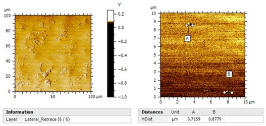
Surface characterization was performed using a commercially available AFM system equipped with a NanoWorld Arrow‑CONTR AFM probe, a silicon cantilever with a force constant of 0.2 N/m, operated in contact mode. Lateral images were used to visualize surface inhomogeneities across the scanned region. The NanoWorld AFM probe ensured stable tip–sample interaction, enabling high‑quality topographical and lateral force mapping. This article emphasizes the importance of selecting a reliable AFM probe for nanoscale membrane characterization.
A reliable replacement of the Olympus®* AC160 –
Optimized Positioning with Maximum AFM Tip Visibility
NanoWorld AG is pleased to introduce the new Arrow-ACR AFM probe, developed to provide research professionals worldwide with a dependable alternative to the discontinued Olympus®* AC160 microcantilever.
The Arrow™ ACR (typical resonance frequency 300 kHz, typical force constant 26 N/m), combines identical mechanical properties as the
Olympus®* AC160 with the well-known Arrow AFM tip and cantilever geometry. Always positioned exactly at the end of the AFM cantilever, this AFM probe offers easy positioning of the AFM tip over the area of interest.
With their moderate stiffness (typical force constant 26 N/m) the Arrow™ ACR probes are particularly suitable for studying relatively soft materials, including various polymers. These AFM probes are designed to perform optimally in non-contact/Tapping™ mode in air, enabling detailed characterization of thin films, coatings, surface roughness, and localized defects.
Users can expect stable operation, high sensitivity and high-speed scanning capabilities, ensuring reproducible data across a wide range of applications.
For researchers seeking a seamless transition from the discontinued
Olympus®* AC160, the NanoWorld® Arrow™ ACR offers a reliable solution backed by NanoWorld’s manufacturing precision and quality control.
A reliable replacement of the Olympus®* AC160 – NanoWorld introduces new Arrow-ACR Silicon AFM probe Optimized Positioning with Maximum AFM Tip Visibility
Until now, diverse polarization structures and topological domains are obtained in ferroelectric thin films or heterostructures, and the polarization switching and subsequent domain nucleation are found to be more conducive to building energy-efficient and multifunctional polarization structures.*
In the article “Ultralow Strain-Induced Emergent Polarization Structures in a Flexible Freestanding BaTiO3 Membrane” Jie Wang, Zhen Liu, Qixiang Wang, Fang Nie, Yanan Chen, Gang Tian, Hong Fang, Bin He, Jinrui Guo, Limei Zheng, Changjian Li, Weiming Lü and Shishen Yan introduce a continuous and periodic strain in a flexible freestanding BaTiO3 membrane to achieve a zigzag morphology. *
The authors successfully fabricated freestanding BTO membranes with a zigzag morphology using the water-solvation process. *
These films exhibited remarkable curvature-dependent long-range coherence and periodic distributions of polarization. Through experiments and phase-field simulations, Jie Wang et al. observed the presence of H–H and T–T polarization boundaries as well as the formation of large-scale chiral vortex domains. *
Interestingly, these singular polar structures could be induced by ultralow uniaxial and biaxial strains (≈0.5%), which is significantly lower than the previously reported values. The accumulation of charge was found to reduce the formation energy, making the singular polar structures more stable. *
This complicated polarization structure resulting from the morphological variation of the ferroelectric domain provides useful insights into the polarization structure and ferroelectric domain under strain engineering. *
The wrinkled ferroelectric oxides with different strained regions and correlated polarization distributions as well as tunable ferroelectricity can pave the way toward novel flexible electronics. *
Understanding the 3D polarization configuration of a wrinkled BTO membrane is crucial for revealing the relationship between the polarization structure and strain distribution.
To evaluate the polarization configuration, piezoresponse force microscopy (PFM) was employed to obtain the piezoresponse under both vertical and lateral modes (referred to as V-PFM and L-PFM, respectively), and the results are shown in Figure 2a from the article by Jie Wang et al. cited in this blogpost. *
The polarization structures in the freestanding wrinkled BTO membrane were characterized by a commercial scanning probe microscope (SPM).
When the conductive AFM probe (NanoWorld Arrow-EFM) with AC bias was in contact with the sample, the sample underwent regular expansions and contractions due to the inverse piezoelectric effect, which caused the AFM probe to oscillate with the sample.
The oscillation amplitude and phase signals were recorded, which corresponded to the piezoresponse strength and polarization orientation, respectively.
Dual AC resonance tracking PFM (DART-PFM) was used to track the shift in the contact resonance frequency caused by the surface roughness, avoid signal crosstalk, obtain more stable piezoelectric signals with higher sensitivity, and ensure the accuracy of data. The vertical deflection and torsional motion of the probe cantilever were used to detect the deformation of the sample, and the IP and OOP polarization components of the sample were obtained.
To determine the domain structures, both the vertical and lateral PFM images were recorded at different sample rotation angles. The local piezoresponse hysteresis loops were measured by fixing the PFM probe on the selected position and then applying a triangular-square waveform, accompanied with a small AC-driven voltage from the probe.
Electrostatic force microscopy (EFM) and scanning Kelvin probe force microscopy (SKPFM) are widely applied to obtain the surface potential of materials through a dual-channel method.
In the Nap mode, the first-line scanning is used to obtain the surface morphology information of the sample, and then the probe is lifted to a certain height to detect the long-range force (electrostatic force) signal. The operating principle of EFM can be simply interpreted as the phase difference imaging of probe vibration caused by the electrostatic force between the probe and sample. In SKPFM, a DC bias is applied to the conductive tip to balance the surface potential of the sample. The DC bias is equal to the potential difference between the tip and sample, thereby obtaining the relative surface potential distribution of the material. Therefore, EFM qualitatively reflects the potential properties of samples, and SKPFM quantifies the potential of samples.*
Figure 2 from Jie Wang et al. (2024), Ultralow Strain-Induced Emergent Polarization Structures in a Flexible Freestanding BaTiO3 Membrane: Domain structures of zigzag-wrinkled BTO film. a) Topographic image of wrinkled BTO film, giving rise to zigzag pattern. V-PFM and L-PFM amplitude and phase images for two different sample rotation angles of 0° and 90°. b) Line profiles of the height, OOP phase, and IP phase (0° and 90°) data (average over 6 pixels) along the red dotted lines in (a). c) Typical OOP and IP phase images overlapped on 3D morphology. The red and blue dotted curves indicate the position of the peak and valley, respectively.
*Jie Wang, Zhen Liu, Qixiang Wang, Fang Nie, Yanan Chen, Gang Tian, Hong Fang, Bin He, Jinrui Guo, Limei Zheng, Changjian Li, Weiming Lü and Shishen Yan Ultralow Strain-Induced Emergent Polarization Structures in a Flexible Freestanding BaTiO3 Membrane
Advanced Science, Volume 11, Issue 25, July 3, 2024, 2401657
DOI: https://doi.org/10.1002/advs.202401657
Open Access The article “Ultralow Strain-Induced Emergent Polarization Structures in a Flexible Freestanding BaTiO3 Membrane” by Jie Wang, Zhen Liu, Qixiang Wang, Fang Nie, Yanan Chen, Gang Tian, Hong Fang, Bin He, Jinrui Guo, Limei Zheng, Changjian Li, Weiming Lü and Shishen Yan is licensed under a Creative Commons Attribution 4.0 International License, which permits use, sharing, adaptation, distribution and reproduction in any medium or format, as long as you give appropriate credit to the original author(s) and the source, provide a link to the Creative Commons license, and indicate if changes were made. The images or other third party material in this article are included in the article’s Creative Commons license, unless indicated otherwise in a credit line to the material. If material is not included in the article’s Creative Commons license and your intended use is not permitted by statutory regulation or exceeds the permitted use, you will need to obtain permission directly from the copyright holder. To view a copy of this license, visit http://creativecommons.org/licenses/by/4.0/.