Over several decades many studies on the reduction of wear of mechanical systems have been conducted.
Methods to reduce wear are generally divided into the following categories: applying lubrication, coating with high-hardness materials, and surface texturing. *
Several studies have reported that coatings with higher hardness show more wear than those with lower hardness. From these reports, it is apparent that wear does not depend solely on the hardness of the surface. Hence, there is a strong motivation for utilizing additional strategies for designing wear-resistive surfaces rather than only enhancing the hardness of the coating. *
In the article “Feasibility of wear reduction for soft nanostructured thin film through enhanced elastic recoverability and contact stress relief” Kuk-Jin Seo, Hyun-Joon Kim and Dae-Eun Kim show, that a soft, thin film comprising randomly aligned carbon nanotubes (CNTs) can reduce surface wear more effectively than a homogeneous thin film because of enhanced elastic recoverability and contact stress relief originating from its mesh structure. *
To investigate the wear characteristics of the mesh structure compared to those of the homogeneous thin film, multi-walled CNTs (MWCNTs) and diamond-like carbon (DLC) thin films were prepared to conduct nanoscale tribological experiments using atomic force microscopy (AFM). The MWCNT thin film showed unmeasurably low wear compared with the DLC thin film under a certain range of normal load. *
To demonstrate the wear reduction mechanism of the MWCNT thin film, its indentation and frictional behaviors were assessed. The indentation behavior of the MWCNT thin film revealed repetitive elastic deformation with a wide strain range and a significantly lower elastic modulus than that of the DLC thin film. The permanent deformation of the MWCNT thin film was observed through frictional experiments under relatively high normal load conditions. *
The presented results are expected to provide insights into the design of highly wear-resistant surfaces using nanostructures. *
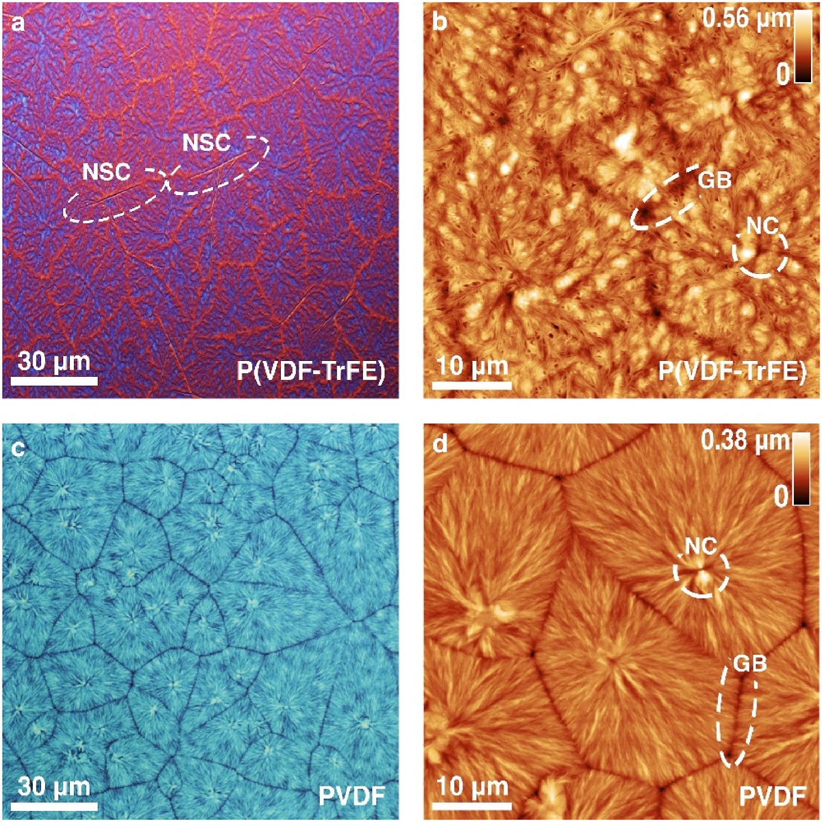
The thickness and surface roughness of the MWCNT and DL thin films were measured using Atomic Force Microscopy. *
The force-displacement (F-D) curves were measured on the MWCNT thin film using the AFM to verify the mechanical behavior when indented by the zirconia microspheres that were used for wear and friction experiments. *
The adhesion forces between the thin films and zirconia microspheres were measured by observing the pull-off force of the F-D curve with the AFM. *
The adhesion force was measured using a colloidal AFM probe to aid the analysis of the tribological characteristics of the thin film. *
The pull-off forces for the DL specimens were obtained at 35 different locations with displacements of 50-200 nm. *
Diamond-coated AFM probes (NanoWorld Pointprobe® DT-NCHR ) were used for scanning, while non-coated silicon AFM probes with relatively high and low spring constants (NanoWorld Pointprobe® NCHR and CONTR) were used for the tribological experiments and specimen characterizations. *

AFM images of wear tracks on the MWCNT thin film under test conditions of (a) 2,000 nN and 20,000 cycles, (b) 6,000 nN and 30,000 cycles, (c) 7,000 nN and 30,000 cycles, (d) 9,200 nN and 30,000 cycles, (e) 13,500 nN and 30,000 cycles, and (f) 28,000 nN and 30,000 cycles. Post-processed AFM images that subtracted the original image before each wear test under conditions of (g) 6,000 nN and 30,000 cycles, (h) 7,000 nN and 30,000 cycles, and (i) 28,000 nN and 30,000 cycles
*Kuk-Jin Seo, Hyun-Joon Kim and Dae-Eun Kim
Feasibility of wear reduction for soft nanostructured thin film through enhanced elastic recoverability and contact stress relief
Friction 11(7): 1292-1306 (2023)
DOI: https://doi.org/10.1007/s40544-022-0669-7
Please follow this external link to read the full article: https://rdcu.be/dejTa
The article “Feasibility of wear reduction for soft nanostructured thin film through enhanced elastic recoverability and contact stress relief” by Kuk-Jin Seo, Hyun-Joon Kim and Dae-Eun Kim is licensed under a Creative Commons Attribution 4.0 International License, which permits use, sharing, adaptation, distribution and reproduction in any medium or format, as long as you give appropriate credit to the original author(s) and the source, provide a link to the Creative Commons license, and indicate if changes were made. The images or other third-party material in this article are included in the article’s Creative Commons license, unless indicated otherwise in a credit line to the material. If material is not included in the article’s Creative Commons license and your intended use is not permitted by statutory regulation or exceeds the permitted use, you will need to obtain permission directly from the copyright holder. To view a copy of this license, visit https://creativecommons.org/licenses/by/4.0/.