Gastric cancer has a high rate of recurrence, and as such, immunotherapy strategies are being investigated as a potential therapeutic strategy. *
Although the involvement of immune checkpoints in immunotherapy is well studied, biomechanical cues, such as target cell stiffness, have not yet been subject to the same level of investigation. *
Changes in the cholesterol content of the cell membrane directly influence tumor cell stiffness. *
In the article “Cholesterol-regulated cellular stiffness may enhance evasion of NK cell-mediated cytotoxicity in gastric cancer stem cells” Lijuan Zhu and Hongjin Wang investigate the effect of cholesterol on NK cell-mediated killing of gastric cancer stem-like cells. *
They report that surviving tumor cells with stem-like properties elevated cholesterol metabolism to evade NK cell cytotoxicity. *
Inhibition of cholesterol metabolism enhances NK cell-mediated killing of gastric cancer stem-like cells, highlighting a potential avenue for improving immunotherapy efficacy. *
This study suggests a possible effect of cancer cell stiffness on immune evasion and offers insights into enhancing immunotherapeutic strategies against tumors. *
Measurement of cell stiffness by AFM:
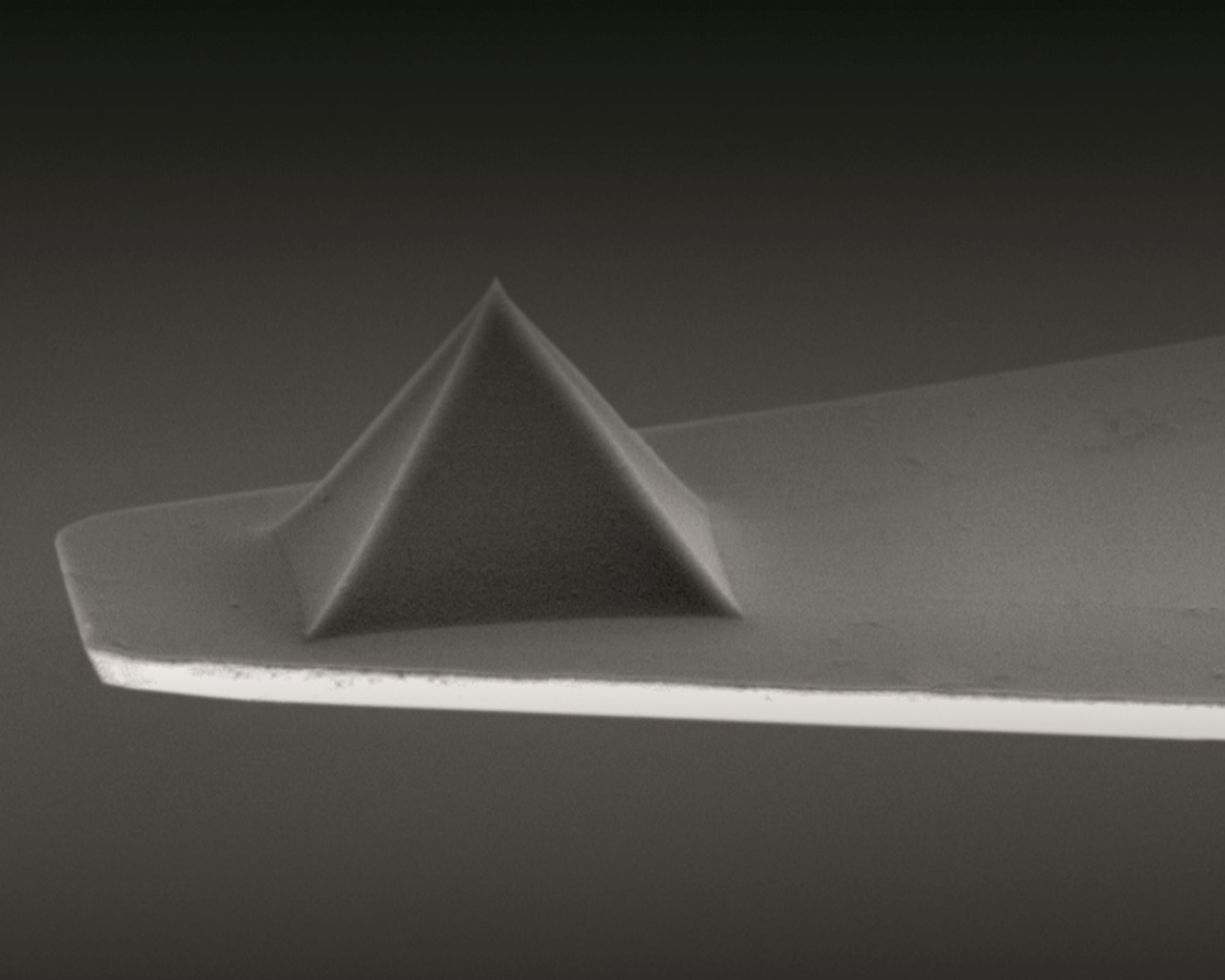
A customized commercially available atomic force microscope (AFM) and NanoWorld Pyrex-Nitride PNP-TR AFM probes were used for the measurement of cell stiffness by AFM. *
Atomic force microscopy cell stiffness was measured according to standard methodology. *
AFM force curves were captured with a customized AFM placed atop an inverted optical microscope that had a heating stage for live-cell imaging and a ×20 objective. Using an XY stage, the materials were moved until the desired cell, which could be observed under an optical microscope, was positioned beneath the AFM tip. Using a NanoWorld PNP-TR-B AFM cantilever (NanoWorld), the force curves on the cell were collected at a rate of ~ 5 μm·s−1 in the relative trigger mode (15 nm trigger threshold). *
By utilizing a thermal tuning and the deflection sensitivity of 170 nm·V−1, the AFM cantilever spring constant was determined to be 0.08 N·m−1. *
Single cells were measured both before and after treatment at 37 °C. The force curves were processed using the AFM’s analysis software, which also computed the Young’s modulus of the sample. This was accomplished by fitting the approach curve to an indentation of less than 500 nm (to account for stiffness) and assuming a cortical Poisson’s ratio of 0.3.*
*Lijuan Zhu and Hongjin Wang
Cholesterol-regulated cellular stiffness may enhance evasion of NK cell-mediated cytotoxicity in gastric cancer stem cells
FEBS Open Bio, Volume 14, Issue 5, May 2024, Pages 855-866
DOI: https://doi.org/10.1002/2211-5463.13793
Open Access The article “Cholesterol-regulated cellular stiffness may enhance evasion of NK cell-mediated cytotoxicity in gastric cancer stem cells” by Lijuan Zhu and Hongjin Wang is licensed under a Creative Commons Attribution 4.0 International License, which permits use, sharing, adaptation, distribution and reproduction in any medium or format, as long as you give appropriate credit to the original author(s) and the source, provide a link to the Creative Commons license, and indicate if changes were made. The images or other third party material in this article are included in the article’s Creative Commons license, unless indicated otherwise in a credit line to the material. If material is not included in the article’s Creative Commons license and your intended use is not permitted by statutory regulation or exceeds the permitted use, you will need to obtain permission directly from the copyright holder. To view a copy of this license, visit http://creativecommons.org/licenses/by/4.0/.
![Figure S2 from Yong Hwee Tan et al. 2024 “Stiffness Mediated-Mechanosensation of Airway Smooth Muscle Cells on Linear Stiffness Gradient Hydrogels”:(A) Correlation of Young’s modulus from macroscale stiffness (UCT) assessment with nanoindentation (AFM), was conducted using cylindrical PA hydrogels of different Acrylamide %/Bis-acrylamide % derived from Tse and Engler [47] 10 %/0.06 %, 10 %/0.1 %, 10 %/0.15 % and 10 %/0.3 % (Linear regression, P < 0.0001, R2 = 0.9288, n = 4). Data are presented as mean SEM. (B) An example force curve from atomic force microscopy with an approach velocity of 2 μm/s, until a 2 nN trigger force was registered, and retraction of indenter at 10 μm/s. NanoWorld triangular Pyrex-Nitride PNP-TR AFM probes were used to assess the stiffness of the hydrogels with atomic force microscopy.](https://www.nanoworld.com/blog/wp-content/uploads/2024/07/Fig-S2-from-Young-Hwee-Tan-2024-Stiffness-Mediated-Mechanosensation-of-Airway-Smooth-Muscle-Cells-on-Linear-Stiffness-Gradient-Hydrogels-NanoWorld-PNP-TR-AFM-probe.jpg)