Synchronized Modulation Kelvin Probe Force Microscopy for Surface Photovoltage Studies in Optoelectronic Systems

Kelvin Probe Force Microscopy (KPFM) has become an essential atomic force microscopy (AFM) technique for investigating surface potentials and charge distributions in electronic and optoelectronic materials. However, conventional KPFM measurements can be affected by thermal drift, probe degradation, and environmental changes during data acquisition, making the accurate characterization of dynamic systems particularly challenging. In this article, Zeinab Eftekhari, Ariane Ufer, Ursula Wurstbauer, and Rebecca Saive introduce synchronized modulation Kelvin probe force microscopy (SM-KPFM), an advanced in-operando approach designed to overcome these limitations.

The authors developed SM-KPFM by synchronizing external stimulus modulation, such as illumination or electrical bias, with the AFM scan direction. In synchronized illumination KPFM, the sample remains unilluminated during the trace scan and illuminated during the retrace scan, enabling direct comparison of surface potential states within the same raster image. This strategy minimizes measurement artifacts arising from drift, thermal effects, and AFM probe degradation while providing highly reproducible surface photovoltage measurements.

The technique was demonstrated on a silicon photodiode and a molybdenum disulfide (MoS₂) bilayer deposited on a gold substrate. By capturing illuminated and non-illuminated contact potential difference (CPD) measurements along identical scan paths, SM-KPFM produced accurate, drift-free surface photovoltage maps and provided improved insight into nanoscale photovoltaic behavior and charge separation processes in optoelectronic materials.

Kelvin Probe Force Microscopy measurements were performed in sideband mode using a NanoWorld ARROW-EFM AFM probe. The Pt/Ir-coated AFM probe, featuring a resonance frequency of 68 kHz and a spring constant of 2.8 N/m, enabled highly sensitive surface potential mapping with excellent electrical conductivity and measurement stability. The synchronization approach required only triggering the illumination source using the AFM scan direction signal, making the technique readily applicable to existing KPFM workflows without complex hardware modifications.

This work demonstrates how combining an innovative synchronized measurement strategy with a NanoWorld ARROW-EFM AFM probe significantly improves the reliability of operando Kelvin Probe Force Microscopy. The methodology opens new opportunities for investigating nanoscale electronic and optoelectronic devices, photovoltaic materials, and other functional nanostructures where precise surface potential mapping is essential.
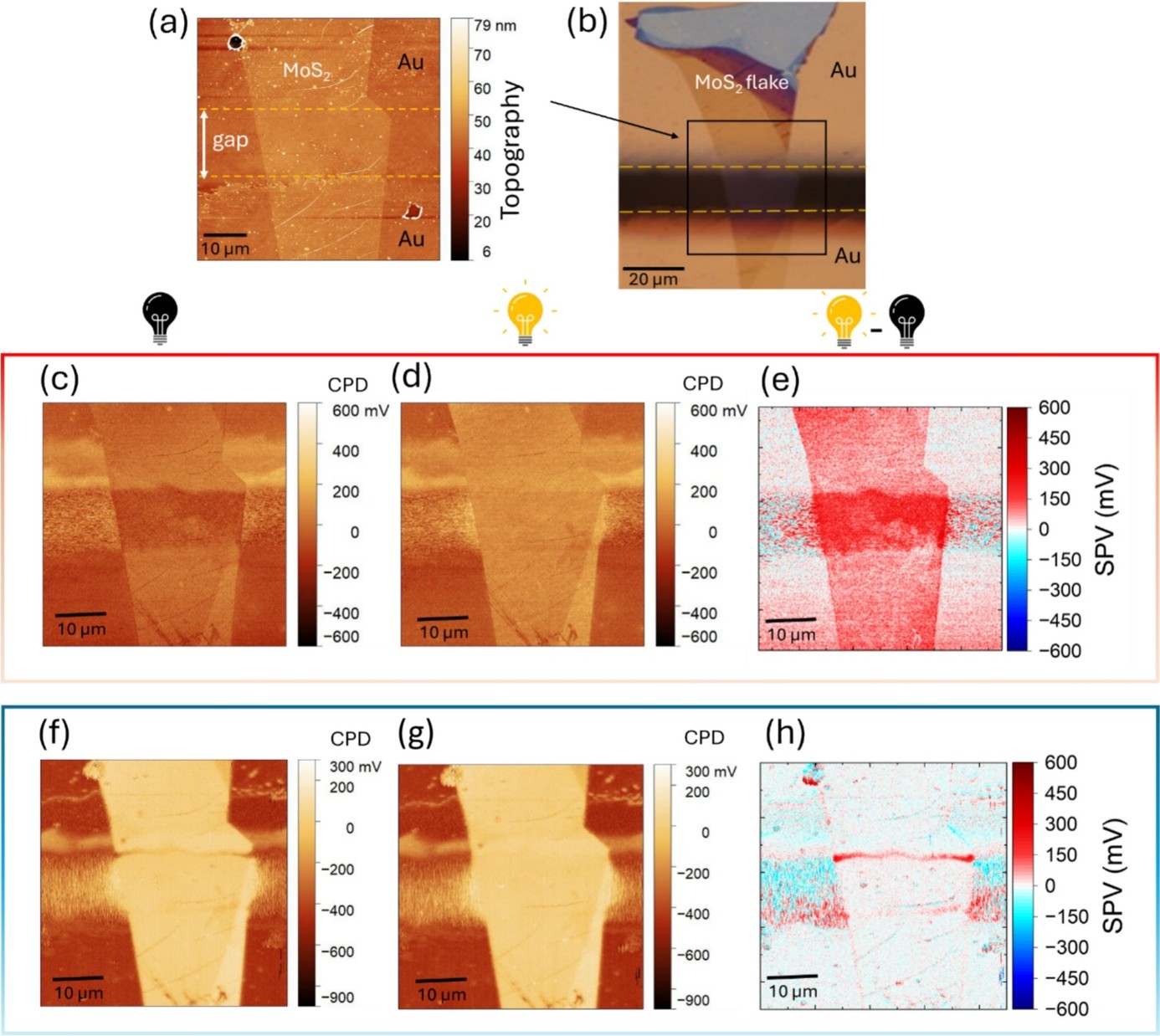
figure 3.
KPFM measurements of a MoS₂ flake on gold electrodes under dark and illuminated conditions. (a) Topography and (b) optical image of the MoS₂ flake on the gold electrodes, where the black box shows the scanned area under AFM/KPFM. The topography image was post-processed to have the substrate and gold contact surfaces on the same level such that the thin flake becomes visible. (c, d) CPD maps acquired in separate scans under dark (c) and illuminated (d) conditions using conventional KPFM (red box). (e) SPV map derived from the sequential scans. (f) Trace (dark) and (g) retrace (illuminated) CPD maps obtained using SM- KPFM (blue box). (h) SPV map (retraced minus trace).

Full citation:
Eftekhari, Z.; Ufer, A.; Wurstbauer, U.; Saive, R.
Synchronized modulation Kelvin probe force microscopy for surface photovoltage studies in optoelectronic systems.
MRS Communications 16 (2026), 180–186.
https://doi.org/10.1557/s43579-025-00899-3
Structural Elucidation of Citric Acid Cross-Linked Pectin and Its Impact on the Properties of Nanocellulose-Reinforced Packaging Films

Citric acid cross-linking is an effective strategy for modifying citrus pectin to enhance its performance in sustainable packaging applications. In this article, Chandra Mohan Chandrasekar, Daniele Carullo, Francesco Saitta, Tommaso Bellesia, Elena Caneva, Chiara Baschieri, Marco Signorelli, Dimitrios Fessas, Stefano Farris and Davide Romano, investigated the structural changes induced by citric acid cross-linking and their influence on the properties of nanocellulose-reinforced packaging films..

The authors demonstrated that cross-linking significantly alters the structure–property relationship of the biopolymer matrix, leading to improved film integrity and modified surface morphology. These results provide valuable insight into biopolymer modification strategies for the development of environmentally friendly packaging materials.

Atomic force microscopy (AFM) was employed to characterize the surface morphology of the films. Measurements were performed using a commercially available AFM instrument operated in contact resonance amplitude imaging (CRAI) mode. A NanoWorld Arrow-FMR AFM probe was used.

This AFM probe features a rectangular beam with a triangular free end and a tetrahedral tip (tip radius ~10 nm, tip height 10–15 μm), with a spring constant of 2.8 N/m and a resonance frequency of 75 kHz. Root mean square surface roughness values were calculated from at least five height-mode images.

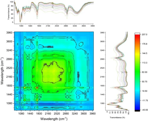
Fig. 3. 2D synchronized correlation analysis of FTIR spectra for CLCP packaging film trials.
Fig. 3. 2D synchronized correlation analysis of FTIR spectra for CLCP packaging film trials. [The intensity of the auto-peaks on the diagonal line represents the overall change in spectral intensity. The key region of interest is the strong auto-peak around 1700 cm−1, highlighted by

Full citation: Chandrasekar, C. M.; Carullo, D.; Saitta, F.; Bellesia, T.; Caneva, E.; Baschieri, C.; Signorelli, M.; Fessas, D.; Farris, S.; Romano, D.
Structural elucidation of citric acid cross-linked pectin and its impact on the properties of nanocellulose-reinforced packaging films.
International Journal of Biological Macromolecules 2025, 333(2), 148869. https://doi.org/10.1016/j.ijbiomac.2025.148869

Attribution 4.0 International By exercising the Licensed Rights (defined below), You accept and agree to be bound by the terms and conditions of this Creative Commons Attribution 4.0 International Public License (“Public License”). To the extent this Public License may be interpreted as a contract, You are granted the Licensed Rights in consideration of Your acceptance of these terms and conditions, and the Licensor grants You such rights in consideration of benefits the Licensor receives from making the Licensed Material available under these terms and conditions. https://creativecommons.org/licenses/by/4.0/legalcode.en

Nonlinear Optical Response in Layer-Stacked Gallenene with Ferroelectric Polarization

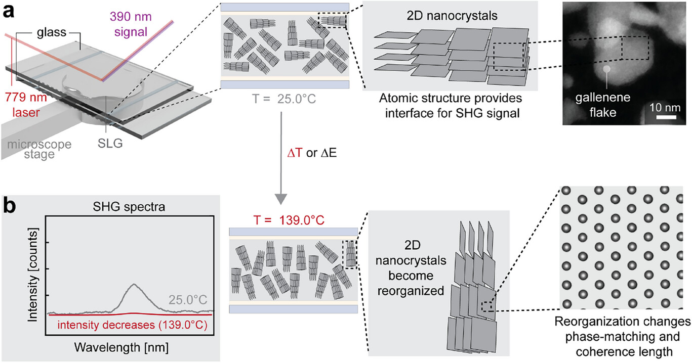
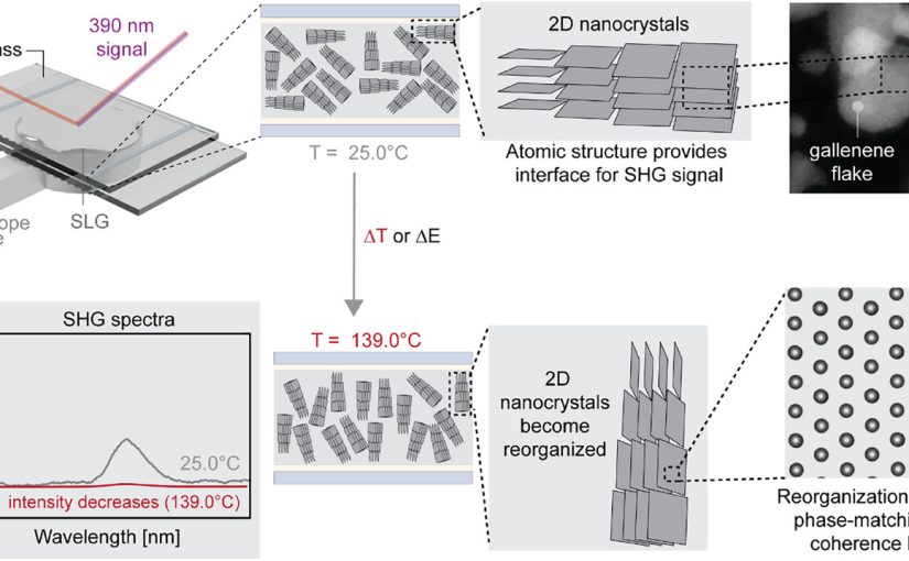
Layer-stacked gallenene is an emerging two-dimensional material with unique structural and electronic propertiesIn this article, M.Yunusa, A. K.Schulz, T.Parker, et al. investigated the nonlinear optical response of layer-stacked gallenene exhibiting ferroelectric polarization. The material was produced using a liquid metal-based synthesis approach and showed a phase transition associated with its stacked structure.

The authors demonstrated strong second harmonic generation (SHG) signals, revealing the nonlinear optical activity of gallenene and confirming its ferroelectric nature. These findings highlight the potential of gallenene as a novel functional 2D material for advanced optoelectronic and photonic applications.

Atomic force microscopy (AFM) was used to characterize transparent lamellar films and helical filaments. Measurements were performed using a commercially available AFM instrument operated in contact mode. A NanoWorld Arrow-CONTR AFM probe with a nominal force constant of 0.2 N/m and a resonance frequency of 14 kHz was used to obtain high-resolution surface morphology data.


Figure 1
Structure of gallenene and complex anatomy of supercooled liquid gallium. Mechanism for electrical and thermal perturbation. a) Illustration of hypothesized interaction of SHG response with SLG in linearly polarized light showing that thermal perturbations could align the 2D nanocrystals, allowing for an increased SHG medium at either temperature or electrical fields. An example HAADF image of gallenene flake sandwiched between two graphene layers, as depicted in (a) (far right microscope image). b) Structural reorganization of gallenene nanocrystals in the SLG leading to an intensity change in SHG signal as a result of thermal or electrical perturbation.

Full citation:

Yunusa, M.; Schulz, A. K.; Parker, T.; Schneider, F.; Elibol, K.; Predel, M.; Dzíbelová, J.; Rebmann, M.; Gorkan, T.; Ye, J.; Tan, J.-C.; Kang, W.; van Aken, P. A.; Meixner, A. J.; Durgun, E.; Kotakoski, J.; Zhang, D.; Sitti, M.
Nonlinear Optical Response in Layer-Stacked Gallenene with Ferroelectric Polarization.
Advanced Materials 2025, 37(44), e01058.
https://doi.org/10.1002/adma.202501058

Attribution 4.0 International By exercising the Licensed Rights (defined below), You accept and agree to be bound by the terms and conditions of this Creative Commons Attribution 4.0 International Public License (“Public License”). To the extent this Public License may be interpreted as a contract, You are granted the Licensed Rights in consideration of Your acceptance of these terms and conditions, and the Licensor grants You such rights in consideration of benefits the Licensor receives from making the Licensed Material available under these terms and conditions. https://creativecommons.org/licenses/by/4.0/