
Synchronized Modulation Kelvin Probe Force Microscopy for Surface Photovoltage Studies in Optoelectronic Systems

Kelvin Probe Force Microscopy (KPFM) has become an essential atomic force microscopy (AFM) technique for investigating surface potentials and charge distributions in electronic and optoelectronic materials. However, conventional KPFM measurements can be affected by thermal drift, probe degradation, and environmental changes during data acquisition, making the accurate characterization of dynamic systems particularly challenging. In this article, Zeinab Eftekhari, Ariane Ufer, Ursula Wurstbauer, and Rebecca Saive introduce synchronized modulation Kelvin probe force microscopy (SM-KPFM), an advanced in-operando approach designed to overcome these limitations.

The authors developed SM-KPFM by synchronizing external stimulus modulation, such as illumination or electrical bias, with the AFM scan direction. In synchronized illumination KPFM, the sample remains unilluminated during the trace scan and illuminated during the retrace scan, enabling direct comparison of surface potential states within the same raster image. This strategy minimizes measurement artifacts arising from drift, thermal effects, and AFM probe degradation while providing highly reproducible surface photovoltage measurements.

The technique was demonstrated on a silicon photodiode and a molybdenum disulfide (MoS₂) bilayer deposited on a gold substrate. By capturing illuminated and non-illuminated contact potential difference (CPD) measurements along identical scan paths, SM-KPFM produced accurate, drift-free surface photovoltage maps and provided improved insight into nanoscale photovoltaic behavior and charge separation processes in optoelectronic materials.

Kelvin Probe Force Microscopy measurements were performed in sideband mode using a NanoWorld ARROW-EFM AFM probe. The Pt/Ir-coated AFM probe, featuring a resonance frequency of 68 kHz and a spring constant of 2.8 N/m, enabled highly sensitive surface potential mapping with excellent electrical conductivity and measurement stability. The synchronization approach required only triggering the illumination source using the AFM scan direction signal, making the technique readily applicable to existing KPFM workflows without complex hardware modifications.

This work demonstrates how combining an innovative synchronized measurement strategy with a NanoWorld ARROW-EFM AFM probe significantly improves the reliability of operando Kelvin Probe Force Microscopy. The methodology opens new opportunities for investigating nanoscale electronic and optoelectronic devices, photovoltaic materials, and other functional nanostructures where precise surface potential mapping is essential.
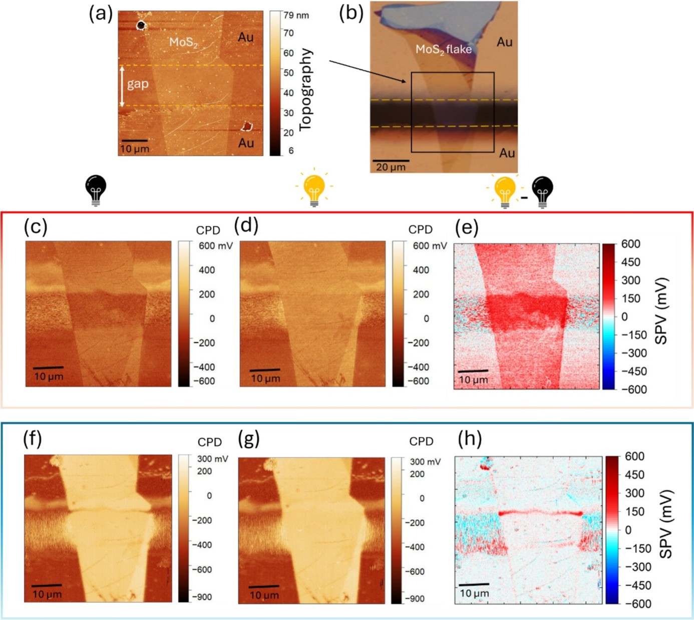
figure 3.
KPFM measurements of a MoS₂ flake on gold electrodes under dark and illuminated conditions. (a) Topography and (b) optical image of the MoS₂ flake on the gold electrodes, where the black box shows the scanned area under AFM/KPFM. The topography image was post-processed to have the substrate and gold contact surfaces on the same level such that the thin flake becomes visible. (c, d) CPD maps acquired in separate scans under dark (c) and illuminated (d) conditions using conventional KPFM (red box). (e) SPV map derived from the sequential scans. (f) Trace (dark) and (g) retrace (illuminated) CPD maps obtained using SM- KPFM (blue box). (h) SPV map (retraced minus trace).

Full citation:
Eftekhari, Z.; Ufer, A.; Wurstbauer, U.; Saive, R.
Synchronized modulation Kelvin probe force microscopy for surface photovoltage studies in optoelectronic systems.
MRS Communications 16 (2026), 180–186.
https://doi.org/10.1557/s43579-025-00899-3
All-ferroelectric implementation of reservoir computing

In the article “All-ferroelectric implementation of reservoir computing”, published in Nature Communications, Zhiwei Chen, Wenjie Li, Shuai Dong, Z. Hugh Fan, Yihong Chen, Xubing Lu, Min Zeng, Minghui Qin, Guofu Zhou, Xingsen Gao, and Jun-Ming Liu report a novel approach for implementing reservoir computing (RC) using a monolithic, fully ferroelectric hardware platform. This work is a result of multidisciplinary collaboration among experts in ferroelectric materials, neuromorphic device engineering, and condensed matter physics.
Reservoir computing is a recurrent neural network model that excels at processing spatiotemporal data, typically requiring complex and heterogeneous hardware. In this study, the authors demonstrate that a single material system—epitaxially grown Pt/BiFeO₃/SrRuO₃ ferroelectric thin films—can simultaneously implement both volatile and nonvolatile functionalities required for RC. This is achieved through precise imprint field (E_imp) engineering, which modifies the polarization dynamics within the ferroelectric layer.
Two types of ferroelectric diodes (FDs) are fabricated from the same stack:
• Volatile FDs, grown at a oxygen pressure of 19 Pa, possess a nonzero imprint field, resulting in spontaneous polarization back-switching after the removal of input pulses. This gives rise to short-term memory and fading dynamics, which are ideal for temporal feature transformation in the reservoir layer.
• Nonvolatile FDs, grown at a oxygen pressure of 15 Pa, with minimal imprint field, exhibit stable long-term potentiation/depression (LTP/LTD), making them well-suited for synaptic weight storage in the readout layer.
The all-ferroelectric RC system was benchmarked on several temporal processing tasks:
• Chaotic Hénon map prediction with a normalized root-mean-square error (NRMSE) of 0.017,
• Waveform classification (NRMSE ≈ 0.13),
• Noisy handwritten digit recognition (up to 91.7% accuracy), and
• Curvature discrimination (100% accuracy).
The devices showed remarkable endurance (>10⁶ cycles), retention (>30 days), low variability (~8% cycle-to-cycle), and extremely low power consumption (~11.8 µW for volatile, ~140 nW for nonvolatile). These results affirm the potential of ferroelectric devices for ultralow-power, scalable neuromorphic computing.
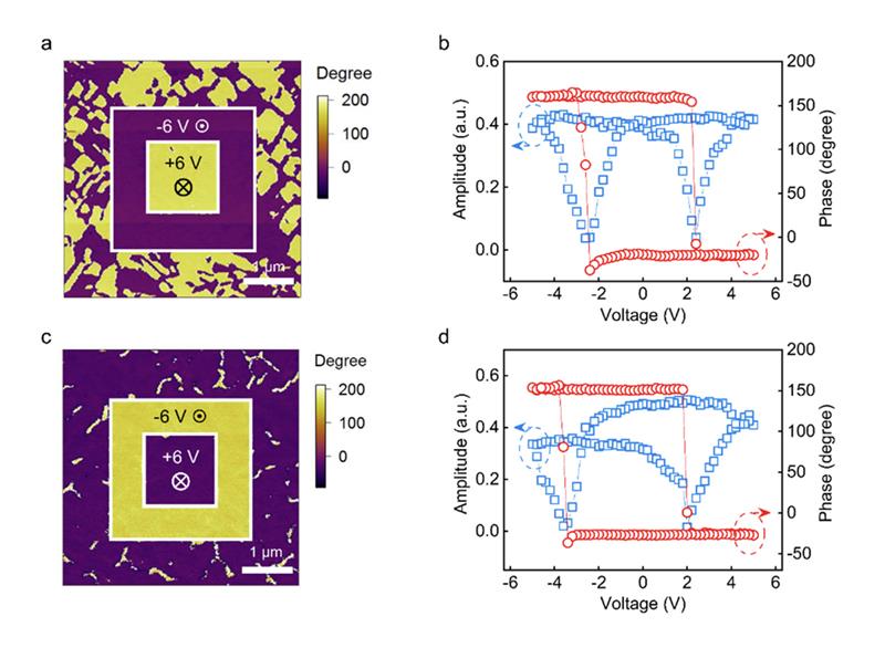
To support these findings, the study employed high-resolution scanning probe microscopy techniques. Specifically, NanoWorld Arrow™ EFM conductive AFM probes were used for piezoresponse force microscopy (PFM). These measurements were critical in confirming that volatility and nonvolatility were governed by tunable imprint fields within the BiFeO₃ layer.
The exceptional electrostatic sensitivity, sharp tip radius, and stable mechanical properties of NanoWorld Arrow™ EFM probes were indispensable in characterizing the field-induced polarization behavior and validating the dual-mode operational framework of the ferroelectric diodes.
This work presents a significant advance in neuromorphic hardware, showing that imprint-field engineering in ferroelectric systems enables the unification of dynamic and static memory functions within a single material system. The integration of volatile and nonvolatile functions into a coherent architecture—combined with robust nanoscale characterization—offers a promising path toward compact, energy-efficient RC platforms based entirely on functional oxides.
Citation:
Chen, Z., Li, W., Dong, S., Fan, Z. H., Chen, Y., Lu, X., Zeng, M., Qin, M., Zhou, G., Gao, X., & Liu, J.-M. (2023). All-ferroelectric implementation of reservoir computing. Nature Communications, 14, 3851. https://doi.org/10.1038/s41467-023-39371-y Read full article here

Figure S3
Figure S3 from the original publication – licensed under CC BY 4.0
Deed – Attribution 4.0 International
– Creative Commons