Plant-Growth Synchronized, Acid Phosphatase-Responsive Lignin-Based Controlled Release Phosphorus Nanofertilizers

Developing smarter fertilizer systems that deliver nutrients when and where plants need them could help improve nutrient efficiency while reducing unnecessary losses to the environment. In this article, Alice Boarino, Nicola Carrara, Joaquin Clua, Nick Zahnd, Yves Poirier, and Harm-Anton Klok present a lignin-based nanofertilizer platform designed to respond to a biological signal associated with phosphate deficiency in plants.

The researchers developed tripolyphosphate (TPP)-cross-linked lignin nanoparticles engineered to release phosphorus in response to acid phosphatase. This enzyme is upregulated by plants under phosphate-starvation conditions, providing a mechanism for synchronizing nutrient release with plant demand. The lignin/TPP nanoparticles therefore combine a biodegradable polymer-based carrier with an enzyme-responsive release mechanism rather than relying on a conventional uncontrolled release process.

The nanofertilizers were prepared from aminated lignin and tripolyphosphate through ionic gelation followed by covalent cross-linking. The resulting nanoparticles were investigated to determine their structural and functional properties and to understand how exposure to acid phosphatase affects their stability. The authors found that phosphorus release was triggered by acid phosphatase activity and occurred together with nanoparticle disintegration, demonstrating the responsiveness of the lignin-based delivery system to the targeted enzymatic stimulus.

The biological experiments further demonstrated the potential of the nanoparticles as a phosphorus source for Arabidopsis thaliana. Treatment with lignin-TPP nanoparticles suppressed the growth inhibition and molecular responses normally associated with phosphate deficiency, supporting their potential as controlled-release nanofertilizers for plant growth and development.

Atomic force microscopy (AFM) was used to characterize the morphology and size distribution of the lignin-based nanoparticles. AFM imaging was performed in tapping mode using a NanoWorld PointProbe® NCSTR-50 AFM probe, an aluminum-coated silicon cantilever with a spring constant of 7.4 N/m and a resonance frequency of approximately 160 kHz.

For AFM analysis, nanoparticle dispersions were deposited onto cleaned silicon wafers and dried overnight at room temperature. Samples prepared in Milli-Q water were used to characterize nanoparticle dimensions, while dispersions in MES buffer were used to investigate the effect of acid phosphatase on nanoparticle stability. The resulting AFM images enabled direct nanoscale characterization of the particles, with nanoparticle sizes determined from the measured particle heights.

The use of a NanoWorld AFM probe in tapping mode provided a suitable approach for imaging these nanoscale polymer-based structures while limiting the interaction between the AFM probe and the deposited nanoparticles. The NanoWorld PointProbe® NCSTR-50 AFM probe therefore played an important role in confirming the morphology and dimensions of the lignin-TPP nanofertilizers.

This work highlights how NanoWorld AFM probes can support nanoscale characterization of responsive polymer nanoparticles and advanced agricultural materials. By combining AFM-based morphological analysis with biochemical response testing and plant experiments, the authors demonstrate a promising approach toward nanofertilizers capable of delivering phosphorus in a plant-growth-synchronized manner.

The study also illustrates the broader potential of nanoscale characterization in the development of responsive agricultural materials, where nanoparticle size, morphology, stability, and stimulus-dependent behavior can all influence the performance of the final delivery system.
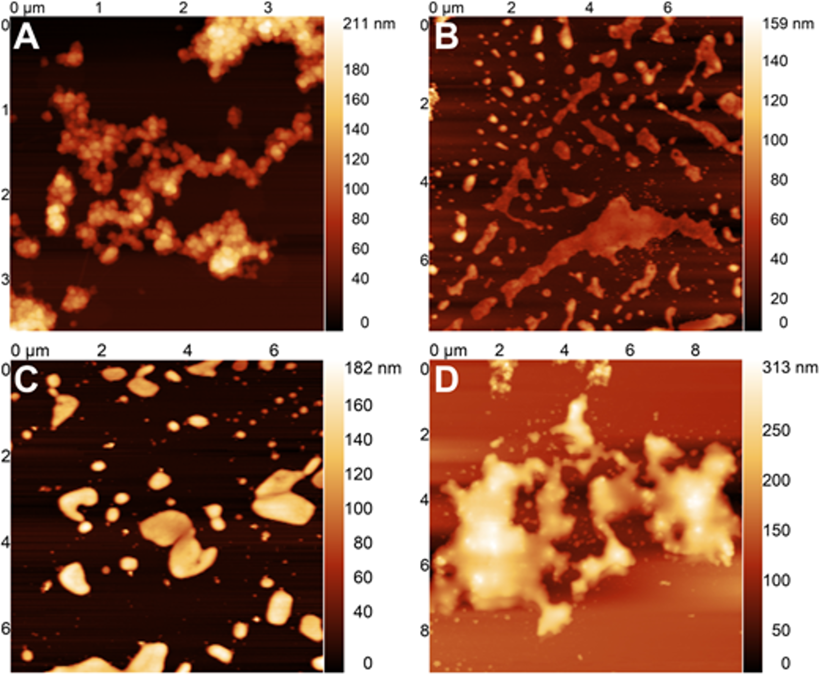
Figure 6.AFM images of cross-linked lignin/TPP nanoparticles after A) 0 h, B) 24 h, C) 48 h, and D) 72 h of incubation with acid phosphatase (10 mU/mL).
Figure 6.
AFM images of cross-linked lignin/TPP nanoparticles after A) 0 h, B) 24 h, C) 48 h, and D) 72 h of incubation with acid phosphatase (10 mU/mL).


Full citation:
Boarino, A.; Carrara, N.; Clua, J.; Zahnd, N.; Poirier, Y.; Klok, H.-A.
Plant-Growth Synchronized, Acid Phosphatase-Responsive Lignin-Based Controlled Release Phosphorus Nanofertilizers.
Biomacromolecules 2026, 27, 5, 3176–3187.
https://doi.org/10.1021/acs.biomac.5c02594

Creative Commons license: CC BY 4.0
Multifunctional Microstructured Surfaces by Microcontact Printing of Reactive Microgels

Engineering surfaces with precisely controlled chemical and structural properties is essential for developing advanced biomaterials, tissue engineering platforms, and biofunctional interfaces. In this article, Inga Litzen, Alexander Töpel, Martin Zenke, Antonio Sechi, and Andrij Pich present a versatile strategy for fabricating multifunctional microstructured surfaces by combining microcontact printing with reactive microgel technology.
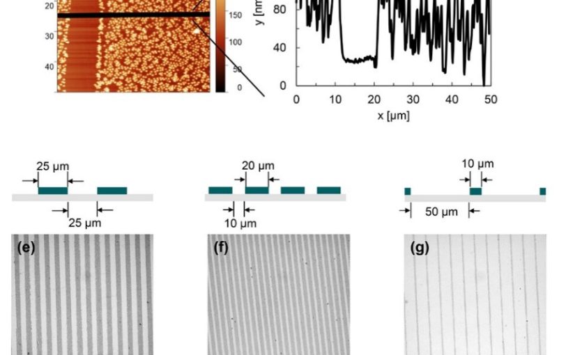
The authors synthesized poly(N-vinylcaprolactam-co-glycidyl methacrylate) (p(VCL-co-GMA)) microgels that serve as functional colloidal inks for microcontact printing onto glass substrates. This approach enabled the fabrication of stable microgel arrays with well-defined geometries and allowed subsequent post-modification with functional molecules, including fluorescent dyes and cell-adhesive peptide sequences. By further introducing controlled surface-chemical gradients through dip-coating, the researchers demonstrated precise spatial control over surface functionality. Cell culture experiments using NIH-3T3 fibroblasts confirmed that peptide-functionalized microgel patterns significantly influenced cell adhesion and migration, highlighting the potential of this platform for bioengineering and regenerative medicine.
Atomic force microscopy (AFM) was employed to characterize the morphology and surface structure of the synthesized microgels after deposition. High-resolution AFM imaging was performed in tapping mode using a NanoWorld PointProbe® NCH AFM probe. The silicon AFM probe, featuring a resonance frequency of approximately 320 kHz and a spring constant of 42 N/m, enabled detailed visualization of the microgel topography and provided valuable information on particle morphology and surface organization at the nanoscale.
AFM characterization complemented dynamic light scattering and zeta potential measurements by providing direct nanoscale imaging of the surface-coated microgels. The high spatial resolution of the NanoWorld PointProbe® NCH AFM probe allowed the authors to verify the successful formation of uniform microgel structures, supporting the optimization of the microcontact printing process and the subsequent surface functionalization steps.

This article demonstrates how NanoWorld AFM probes contribute to the characterization of advanced polymeric microgel systems used for surface engineering. By combining high-resolution AFM imaging with microcontact printing and post-functionalization strategies, the study provides new opportunities for designing multifunctional surfaces for biomedical, biotechnology, and materials science applications.

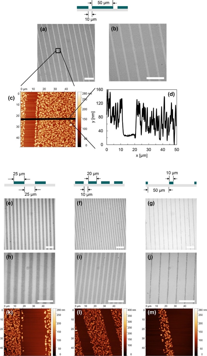
Figure 3Imaging of surfaces structured with p(VCL-co-10mol%GMA-shell) microgels via microcontact printing. a,b,e-j) Light microscopy images and c,k-m) AFM images were recorded. Additionally, d) shows a height profile generated from the AFM image b). The ideal dimensions of resulting patterns are given in the schemes above. Dark grey areas in light microscopy images represent microgel stripes, lighter areas represent the bare glass. Scale bars in light microscopy images: 100 µm.
Figure 3
Imaging of surfaces structured with p(VCL-co-10mol%GMA-shell) microgels via microcontact printing. a,b,e-j) Light microscopy images and c,k-m) AFM images were recorded. Additionally, d) shows a height profile generated from the AFM image b). The ideal dimensions of resulting patterns are given in the schemes above. Dark grey areas in light microscopy images represent microgel stripes, lighter areas represent the bare glass. Scale bars in light microscopy images: 100 µm.

Full citation:
Litzen, I.; Töpel, A.; Zenke, M.; Sechi, A.; Pich, A.
Multifunctional Microstructured Surfaces by Microcontact Printing of Reactive Microgels.
Advanced Functional Materials 36(15), e16135 (2026).
https://doi.org/10.1002/adfm.202516135

Creative Commons license: CC BY 4.0
Synchronized Modulation Kelvin Probe Force Microscopy for Surface Photovoltage Studies in Optoelectronic Systems

Kelvin Probe Force Microscopy (KPFM) has become an essential atomic force microscopy (AFM) technique for investigating surface potentials and charge distributions in electronic and optoelectronic materials. However, conventional KPFM measurements can be affected by thermal drift, probe degradation, and environmental changes during data acquisition, making the accurate characterization of dynamic systems particularly challenging. In this article, Zeinab Eftekhari, Ariane Ufer, Ursula Wurstbauer, and Rebecca Saive introduce synchronized modulation Kelvin probe force microscopy (SM-KPFM), an advanced in-operando approach designed to overcome these limitations.

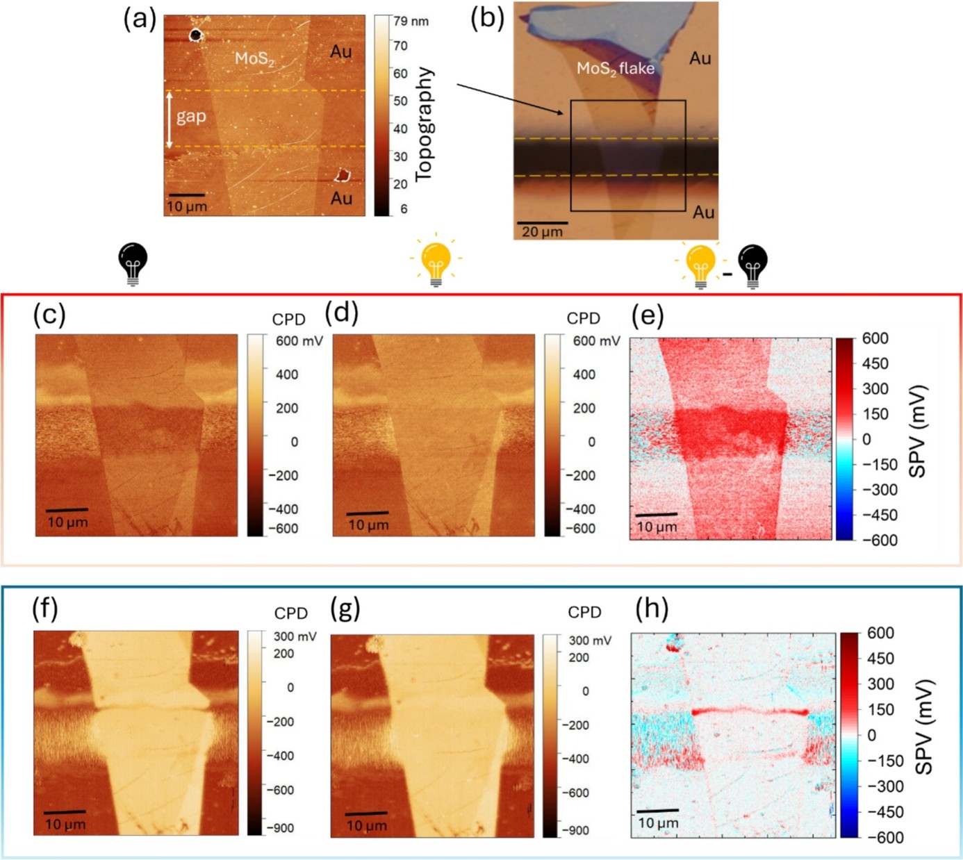
The authors developed SM-KPFM by synchronizing external stimulus modulation, such as illumination or electrical bias, with the AFM scan direction. In synchronized illumination KPFM, the sample remains unilluminated during the trace scan and illuminated during the retrace scan, enabling direct comparison of surface potential states within the same raster image. This strategy minimizes measurement artifacts arising from drift, thermal effects, and AFM probe degradation while providing highly reproducible surface photovoltage measurements.

The technique was demonstrated on a silicon photodiode and a molybdenum disulfide (MoS₂) bilayer deposited on a gold substrate. By capturing illuminated and non-illuminated contact potential difference (CPD) measurements along identical scan paths, SM-KPFM produced accurate, drift-free surface photovoltage maps and provided improved insight into nanoscale photovoltaic behavior and charge separation processes in optoelectronic materials.

Kelvin Probe Force Microscopy measurements were performed in sideband mode using a NanoWorld ARROW-EFM AFM probe. The Pt/Ir-coated AFM probe, featuring a resonance frequency of 68 kHz and a spring constant of 2.8 N/m, enabled highly sensitive surface potential mapping with excellent electrical conductivity and measurement stability. The synchronization approach required only triggering the illumination source using the AFM scan direction signal, making the technique readily applicable to existing KPFM workflows without complex hardware modifications.

This work demonstrates how combining an innovative synchronized measurement strategy with a NanoWorld ARROW-EFM AFM probe significantly improves the reliability of operando Kelvin Probe Force Microscopy. The methodology opens new opportunities for investigating nanoscale electronic and optoelectronic devices, photovoltaic materials, and other functional nanostructures where precise surface potential mapping is essential.

figure 3.
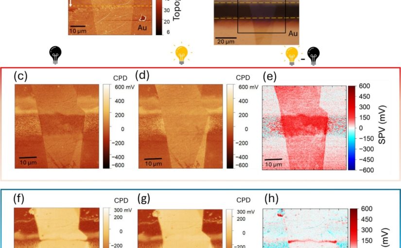
KPFM measurements of a MoS₂ flake on gold electrodes under dark and illuminated conditions. (a) Topography and (b) optical image of the MoS₂ flake on the gold electrodes, where the black box shows the scanned area under AFM/KPFM. The topography image was post-processed to have the substrate and gold contact surfaces on the same level such that the thin flake becomes visible. (c, d) CPD maps acquired in separate scans under dark (c) and illuminated (d) conditions using conventional KPFM (red box). (e) SPV map derived from the sequential scans. (f) Trace (dark) and (g) retrace (illuminated) CPD maps obtained using SM- KPFM (blue box). (h) SPV map (retraced minus trace).

Full citation:
Eftekhari, Z.; Ufer, A.; Wurstbauer, U.; Saive, R.
Synchronized modulation Kelvin probe force microscopy for surface photovoltage studies in optoelectronic systems.
MRS Communications 16 (2026), 180–186.
https://doi.org/10.1557/s43579-025-00899-3