Fabrication of Thin-Film Composite Nanofiltration Membrane Employing Polyelectrolyte and Metal–Organic Framework (MOF) via Spin-Spray-Assisted Layer-by-Layer Assembly

Spin‑spray‑assisted layer‑by‑layer (LbL) assembly is an innovative technique for producing nanostructured thin films due to its rapid deposition and excellent substrate coverage. In this article, Farid Fadhillah fabricated a nanofiltration (NF) membrane composed of multilayers of polyethyleneimine (PEI) and poly(sodium‑4‑styrene sulfonate) (PSS) on a polysulfone (PSF) support. The resulting membrane was subsequently coated with a metal–organic framework (MOF303).
The fabricated (PEI/PSS)₅–MOF303 membrane demonstrated a rejection rate of 18.94 ± 1.58% and a permeability of 0.91 ± 0.13 L/(h·bar·m²), while also exhibiting improved antifouling performance. These findings highlight the potential of spin‑spray‑assisted LbL assembly as a promising route for thin‑film composite membrane fabrication.
Surface characterization was performed using a commercially available AFM system equipped with a NanoWorld Arrow‑CONTR AFM probe, a silicon cantilever with a force constant of 0.2 N/m, operated in contact mode. Lateral images were used to visualize surface inhomogeneities across the scanned region. The NanoWorld AFM probe ensured stable tip–sample interaction, enabling high‑quality topographical and lateral force mapping. This article emphasizes the importance of selecting a reliable AFM probe for nanoscale membrane characterization.
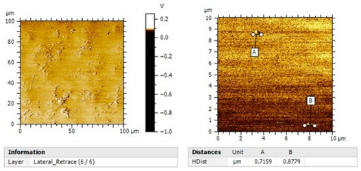
4. Atomic Force Microscope image ((left): lateral retrace (scan size 100 × 100 μm), (right): particle size (scan size: 10 × 10 μm)).

Full Citation:

Farid Fadhillah
Fabrication of Thin-Film Composite Nanofiltration Membrane Employing Polyelectrolyte and Metal–Organic Framework (MOF) via Spin-Spray-Assisted Layer-by-Layer Assembly.
Engineering Proceedings, 2025, 105(1). DOI: https://doi.org/10.3390/engproc2025105003

The article “Fabrication of Thin-Film Composite Nanofiltration Membrane Employing Polyelectrolyte and Metal–Organic Framework (MOF) via Spin-Spray-Assisted Layer-by-Layer Assemblyis published under the Creative Commons Attribution (CC BY) license, which permits unrestricted use, distribution, and reproduction in any medium, provided the original author and source are credited. If material is not included in the article’s Creative Commons license and your intended use is not permitted by statutory regulation or exceeds the permitted use, you will need to obtain permission directly from the copyright holder. To view a copy of this license, visit http://creativecommons.org/licenses/by/4.0/.
Nonlinear Optical Response in Layer-Stacked Gallenene with Ferroelectric Polarization

Layer-stacked gallenene is an emerging two-dimensional material with unique structural and electronic propertiesIn this article, M.Yunusa, A. K.Schulz, T.Parker, et al. investigated the nonlinear optical response of layer-stacked gallenene exhibiting ferroelectric polarization. The material was produced using a liquid metal-based synthesis approach and showed a phase transition associated with its stacked structure.

The authors demonstrated strong second harmonic generation (SHG) signals, revealing the nonlinear optical activity of gallenene and confirming its ferroelectric nature. These findings highlight the potential of gallenene as a novel functional 2D material for advanced optoelectronic and photonic applications.

Atomic force microscopy (AFM) was used to characterize transparent lamellar films and helical filaments. Measurements were performed using a commercially available AFM instrument operated in contact mode. A NanoWorld Arrow-CONTR AFM probe with a nominal force constant of 0.2 N/m and a resonance frequency of 14 kHz was used to obtain high-resolution surface morphology data.


Figure 1
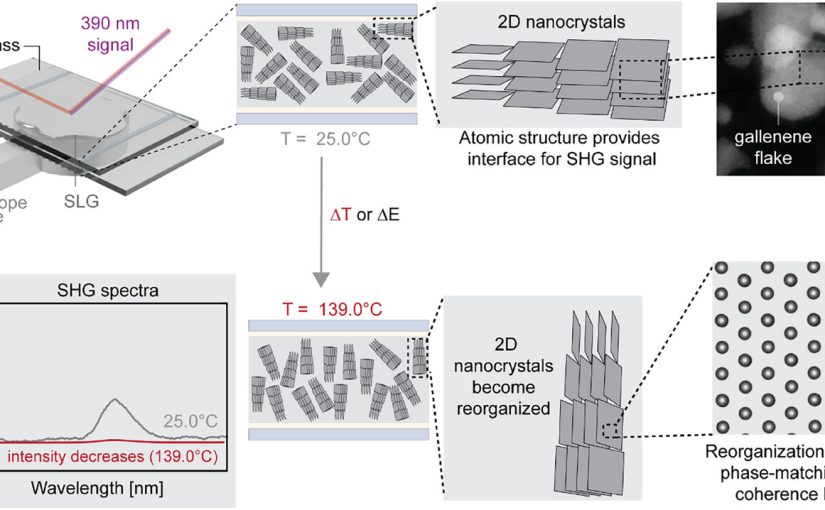
Structure of gallenene and complex anatomy of supercooled liquid gallium. Mechanism for electrical and thermal perturbation. a) Illustration of hypothesized interaction of SHG response with SLG in linearly polarized light showing that thermal perturbations could align the 2D nanocrystals, allowing for an increased SHG medium at either temperature or electrical fields. An example HAADF image of gallenene flake sandwiched between two graphene layers, as depicted in (a) (far right microscope image). b) Structural reorganization of gallenene nanocrystals in the SLG leading to an intensity change in SHG signal as a result of thermal or electrical perturbation.

Full citation:

Yunusa, M.; Schulz, A. K.; Parker, T.; Schneider, F.; Elibol, K.; Predel, M.; Dzíbelová, J.; Rebmann, M.; Gorkan, T.; Ye, J.; Tan, J.-C.; Kang, W.; van Aken, P. A.; Meixner, A. J.; Durgun, E.; Kotakoski, J.; Zhang, D.; Sitti, M.
Nonlinear Optical Response in Layer-Stacked Gallenene with Ferroelectric Polarization.
Advanced Materials 2025, 37(44), e01058.
https://doi.org/10.1002/adma.202501058

Attribution 4.0 International By exercising the Licensed Rights (defined below), You accept and agree to be bound by the terms and conditions of this Creative Commons Attribution 4.0 International Public License (“Public License”). To the extent this Public License may be interpreted as a contract, You are granted the Licensed Rights in consideration of Your acceptance of these terms and conditions, and the Licensor grants You such rights in consideration of benefits the Licensor receives from making the Licensed Material available under these terms and conditions. https://creativecommons.org/licenses/by/4.0/


Optimized positioning through maximized tip visibility – Arrow AFM probes screencast passes 500 views mark

The screencast about NanoWorld Arrow Silicon AFM probes held byNanoWorld AG CEO Manfred Detterbeck has just passed the 500 views mark. Congratulations Manfred!

NanoWorld Arrow™ AFM probes are designed for easy AFM tip positioning and high resolution AFM imaging and are very popular with AFM users due to the highly symetric scans that are possible with these AFM probes because of their special tip shape. They fit to all well-known commercial SPMs (Scanning Probe Microscopes) and AFMs (Atomic Force Microscopes). The Arrow AFM probe consists of an AFM probe support chip with an AFM cantilever which has a tetrahedral AFM tip at its triangular free end.

The Arrow AFM probe is entirely made of monolithic, highly doped silicon.

The unique Arrow™ shape of the AFM cantilever with the AFM tip always placed at the very end of the AFM cantilever allows easy positioning of the AFM tip on the area of interest.
The Arrow AFM probes are available for non-contact mode, contact mode and force modulation mode imaging and are also available with a conductive platinum iridum coating. Furthermore the Arrow™ AFM probe series also includes a range of tipless AFM cantilevers and AFM cantilever arrays as well as dedicated ultra-high frequency Arrow AFM probes for high speed AFM.

To find out more about the different variations please have a look at:

https://www.nanoworld.com/arrow-afm-tips

You can also find various application examples for the Arrow AFM probes in the NanoWorld blog. For a selection of these articles just click on the “Arrow AFM probes” tag on the bottom of this blog entry.