Studying the cation dependence of CO2 reduction intermediates at Cu by in situ VSFG spectroscopy

The nature of the electrolyte cation is known to have a significant impact on electrochemical reduction of CO2 at catalyst|electrolyte interfaces. An understanding of the underlying mechanism responsible for catalytic enhancement as the alkali metal cation group is descended is key to guide catalyst development. *

In the article “Studying the cation dependence of CO2 reduction intermediates at Cu by in situ VSFG spectroscopy” Liam C. Banerji, Hansaem Jang, Adrian M. Gardner and Alexander J. Cowan use in situ vibrational sum frequency generation (VSFG) spectroscopy to monitor changes in the binding modes of the CO intermediate at the electrochemical interface of a polycrystalline Cu electrode during CO2 reduction as the electrolyte cation is varied.  *

Three alkali metal cations have been chosen for analysis: K+, which is the most commonly used electrolyte cation for eCO2R, Cs+, which has been shown to give the greatest enhancement for C2+ products, and Na+, which shows poorer eCO2R performance than K+ whilst maintaining appreciable levels of C-based products. The ability of VSFG to study catalyst|electrolyte interfaces without the need for modifications, as required in the spectroelectrochemical studies mentioned in the article, which can fundamentally alter the electrodes activity, makes it an important tool to assess the mechanisms occurring on the pc-Cu electrodes routinely employed for eCO2R. *

A CObridge mode is observed only when using Cs+, a cation that is known to facilitate CO2 reduction on Cu, supporting the proposed involvement of CObridge sites in CO coupling mechanisms during CO2 reduction. Ex situ measurements show that the cation dependent CObridge modes correlate with morphological changes of the Cu surface. *

The results presented in the article suggest that a high level of bridge site formation is related to, or facilitated by, the Cu restructuring that happens as a result of the use of the Cs+ cations in the supporting electrolyte. Recent reports have indicated that multiple (bridge) bound CO may be electrochemically inert but this work builds on the emerging evidence that CObridge sites are a key intermediate in the CO–CO coupling step that is required for C2+ formation during eCO2R. *

NanoWorld Pointprobe® CONTR AFM probes for contact mode atomic force microscopy (AFM) were used to characterize the morphology of the CU electrode surface before bulk electrolysis and after bulk electrolysis.*

Fig. 5 from Liam C. Banerji et al. “Studying the cation dependence of CO2 reduction intermediates at Cu by in situ VSFG spectroscopy”: AFM images showing surface morphology of the Cu electrode surface (a) before bulk electrolysis, after bulk electrolysis in CO2 purged 0.5 M (b) NaHCO3, (c) KHCO3 and (d) CsHCO3 and also in (e) CO purged 0.5 M CsHCO3. Image analysis methods are described in the Experimental section.NanoWorld Pointprobe® CONTR AFM probes for contact mode atomic force microscopy (AFM) were used to characterize the morphology of the CU electrode surface before bulk electrolysis and after bulk electrolysis.
Fig. 5 from Liam C. Banerji et al. “Studying the cation dependence of CO2 reduction intermediates at Cu by in situ VSFG spectroscopy”: AFM images showing surface morphology of the Cu electrode surface (a) before bulk electrolysis, after bulk electrolysis in CO2 purged 0.5 M (b) NaHCO3, (c) KHCO3 and (d) CsHCO3 and also in (e) CO purged 0.5 M CsHCO3. Image analysis methods are described in the Experimental section of the original article.

*Liam C. Banerji, Hansaem Jang, Adrian M. Gardner and Alexander J. Cowan
Studying the cation dependence of CO2 reduction intermediates at Cu by in situ VSFG spectroscopy
Chemical Science 2024, 15, 2889-2897
DOI:   https://doi.org/10.1039/D3SC05295H

The article “Studying the cation dependence of CO2 reduction intermediates at Cu by in situ VSFG spectroscopy” by Liam C. Banerji, Hansaem Jang, Adrian M. Gardner and Alexander J. Cowan is licensed under a Creative Commons Attribution 3.0 International License, which permits use, sharing, adaptation, distribution and reproduction in any medium or format, as long as you give appropriate credit to the original author(s) and the source, provide a link to the Creative Commons license, and indicate if changes were made. The images or other third-party material in this article are included in the article’s Creative Commons license, unless indicated otherwise in a credit line to the material. If material is not included in the article’s Creative Commons license and your intended use is not permitted by statutory regulation or exceeds the permitted use, you will need to obtain permission directly from the copyright holder. To view a copy of this license, visit https://creativecommons.org/licenses/by/3.0/.

Piezoelectric property of PZT nanofibers characterized by resonant piezo-force microscopy

Nano-piezoelectric materials such as 1D piezoelectric nanofibers, nanowires, and nanobelts have attracted a lot of research interest in recent years. *

Because of their active property that can transform strain energy into electricity, 1D piezoelectric nano-materials can be building blocks for nano-generators, strain sensors, acoustic sensors, force sensors, biosensors, self-powered drug delivery systems, piezoelectric transistors and other intelligent systems. *

The most important property of these active materials is their ability to convert mechanical energy into electrical energy and vice versa. *

Therefore, researchers started developing nano-sized piezoelectric materials in hope of achieving better piezoelectric properties. *

The characterization of these piezoelectric properties, especially measuring the piezoelectric strain coefficients, remains a challenge. *

The Atomic Force Microscopy (AFM)-based method to directly measure nano-materials’ piezoelectric strain coefficients is widely used.

However, several factors such as the extremely small piezoelectric deformation, the influence from the parasitic electrostatic force, and the environmental noise can make the measurement results questionable. *

In the article “Piezoelectric property of PZT nanofibers characterized by resonant piezo-force microscopy” Guitao Zhang, Xi Chen, Weihe Xu, Wei-Dong Yao, and Yong Shi address these issues by introducing a resonant piezo-force microscopy method and describing how it was used to accurately measure the piezoelectric deformation from 1D piezoelectric nanofibers. *

During the measurement the AFM tip was brought into contact with the piezoelectric sample and set to work close to the AFM tip’s first resonant frequency. *

The AFM probe used in this test was a platinum iridium coated NanoWorld Arrow-CONTPt (typical force constant 0.2 N/m, typical resonant frequency 14 KHz. The PtIr coating makes the AFM tip conductive and at the same time enhances the laser reflection from the detector facing side of the AFM cantilever to the photodetector. *

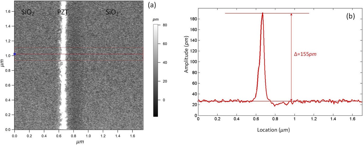
A lock-in amplifier was used to pick up the sample’s deformation signal at the testing frequency. By using this technique, the piezoelectric strain constant d33 of the Lead Zirconate Titanate (PZT) nanofiber with a diameter of 76 nm was measured. The result showed that d33 of this PZT nanofiber was around 387 pm/V. Meanwhile, by tracking the piezoelectric deformation phase image, domain structures inside PZT nanofibers were identified. *

Figure 5 from “Piezoelectric property of PZT nanofibers characterized by resonant piezo-force microscopy” by Guitao Zhang et al. : Piezoelectric deformation amplitude image from a PZT nanofiber on a silicon dioxide substrate (a) and its cross-sectional view along the horizontal direction (b). Conductive NanoWorld Arrow-CONTPt AFM probes were used for the resonant piezo-force microscopy
Figure 5 from “Piezoelectric property of PZT nanofibers characterized by resonant piezo-force microscopy” by Guitao Zhang et al. :
Piezoelectric deformation amplitude image from a PZT nanofiber on a silicon dioxide substrate (a) and its cross-sectional view along the horizontal direction (b).


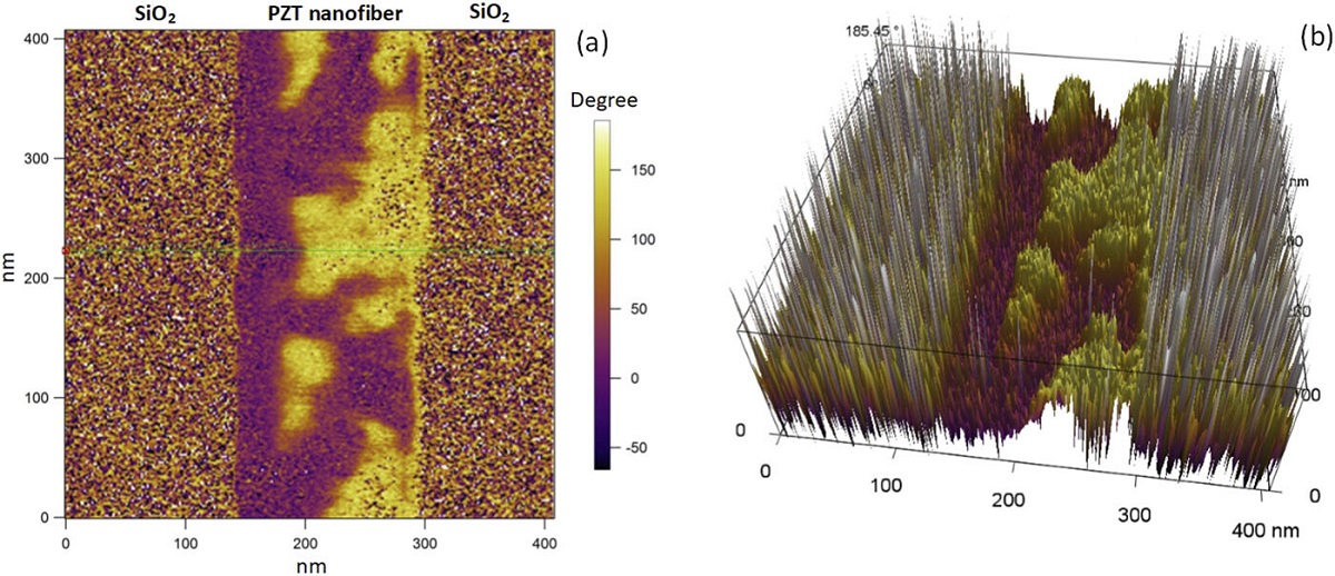
Figure 6 from “Piezoelectric property of PZT nanofibers characterized by resonant piezo-force microscopy” by Guitao Zhang et al. : (a) Piezoelectric deformation phase image from a PZT nanofiber on the silicon dioxide substrate and its 3D image (b). NanoWorld Arrow-CONTPt platinum iridium 5 coated AFM probes were used.
Figure 6 from “Piezoelectric property of PZT nanofibers characterized by resonant piezo-force microscopy” by Guitao Zhang et al. :
(a) Piezoelectric deformation phase image from a PZT nanofiber on the silicon dioxide substrate and its 3D image (b).

*Guitao Zhang, Xi Chen, Weihe Xu, Wei-Dong Yao and Yong Shi
Piezoelectric property of PZT nanofibers characterized by resonant piezo-force microscopy
AIP Advances 12, 035203 (2022)
DOI: https://doi.org/10.1063/5.0081109

The article “Piezoelectric property of PZT nanofibers characterized by resonant piezo-force microscopy” by Guitao Zhang, Xi Chen, Weihe Xu, Wei-Dong Yao and Yong Shi is licensed under a Creative Commons Attribution 4.0 International License, which permits use, sharing, adaptation, distribution and reproduction in any medium or format, as long as you give appropriate credit to the original author(s) and the source, provide a link to the Creative Commons license, and indicate if changes were made. The images or other third party material in this article are included in the article’s Creative Commons license, unless indicated otherwise in a credit line to the material. If material is not included in the article’s Creative Commons license and your intended use is not permitted by statutory regulation or exceeds the permitted use, you will need to obtain permission directly from the copyright holder. To view a copy of this license, visit https://creativecommons.org/licenses/by/4.0/.

Optimized positioning through maximized tip visibility – Arrow AFM probes screencast passes 500 views mark

The screencast about NanoWorld Arrow Silicon AFM probes held byNanoWorld AG CEO Manfred Detterbeck has just passed the 500 views mark. Congratulations Manfred!

NanoWorld Arrow™ AFM probes are designed for easy AFM tip positioning and high resolution AFM imaging and are very popular with AFM users due to the highly symetric scans that are possible with these AFM probes because of their special tip shape. They fit to all well-known commercial SPMs (Scanning Probe Microscopes) and AFMs (Atomic Force Microscopes). The Arrow AFM probe consists of an AFM probe support chip with an AFM cantilever which has a tetrahedral AFM tip at its triangular free end.

The Arrow AFM probe is entirely made of monolithic, highly doped silicon.

The unique Arrow™ shape of the AFM cantilever with the AFM tip always placed at the very end of the AFM cantilever allows easy positioning of the AFM tip on the area of interest.
The Arrow AFM probes are available for non-contact mode, contact mode and force modulation mode imaging and are also available with a conductive platinum iridum coating. Furthermore the Arrow™ AFM probe series also includes a range of tipless AFM cantilevers and AFM cantilever arrays as well as dedicated ultra-high frequency Arrow AFM probes for high speed AFM.

To find out more about the different variations please have a look at:

https://www.nanoworld.com/arrow-afm-tips

You can also find various application examples for the Arrow AFM probes in the NanoWorld blog. For a selection of these articles just click on the “Arrow AFM probes” tag on the bottom of this blog entry.