Type: DT-NCHR

Diamond coated AFM tip - Non-contact / Tapping™ mode - High resonance frequency - Reflex coating

Logo
Cantilever Data Value Range*
Resonance Frequency 400 kHz 280 - 510 kHz
Force Constant 80 N/m 42 - 142 N/m
Length 125 µm 120 - 130 µm
Mean Width 30 µm 25 - 35 µm
Thickness 4 µm 3.5 - 4.5 µm

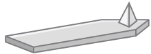
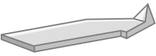
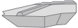
This AFM probe has alignment grooves on the back side of the support chip.
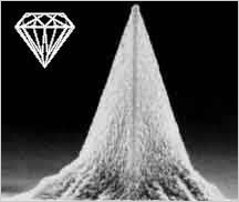
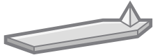
diamond coated tip

diamond coated tip

Product Description

NanoWorld® Pointprobe® NCH probes are designed for non-contact or tapping mode imaging. This AFM probe type combines high operation stability with outstanding sensitivity and fast scanning ability.

All AFM probes of the Pointprobe® series are made from monolithic silicon which is highly doped to dissipate static charge. They are chemically inert and offer a high mechanical Q-factor for high sensitivity. The AFM tip is shaped like a polygon based pyramid with a typical height of 10 - 15 µm.

For applications that require hard contact between AFM tip and sample this AFM probe offers a real diamond tip-side coating. This coating features extremely high wear resistance due to the unsurpassed hardness of diamond.

The typical macroscopic AFM tip radius of curvature lies in the range between 100 and 200 nm. Nanoroughnesses in the 10 nm regime improve the resolution on flat surfaces.

For applications requiring lower resonance frequencies or an AFM cantilever length exceeding 125 µm we recommend our Pointprobe® type DT-NCLR.

Image 
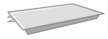
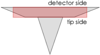
A trapezoidal cross section of the AFM cantilever and therefore 30% wider (e.g. NCH) AFM cantilever detector side result in easier and faster laser adjustment. Additionally, because there is simply more space to place and reflect the laser beam, a higher SUM signal is reached.

Tip shape: Standard

Coating: Diamond

Diamond Coating / Aluminum Reflex Coating

The diamond coating consists of a 100 nm thick polycrystalline diamond layer deposited on the tip side of the AFM cantilever resulting in an unsurpassed hardness of the AFM tip.

The aluminum reflex coating deposited on the detector side of the AFM cantilever enhances the reflectance of the laser beam and prevents light from interfering within the AFM cantilever.

Order Codes

Order Code Quantity Data Sheet
DT-NCHR-10 10 yes
DT-NCHR-20 20 yes
DT-NCHR-50 50 no

NanoWorld® Pointprobe® Diamond Coated AFM Tip (DT), Conductive Diamond Coated AFM Tip (CDT) Screencast

Subscribe to NanoWorld® Youtube Channel

Bruker® is a trademark of Bruker Corporation

Scientific publications mentioning use of this AFM probe


Saha A, Kim Y, Kim KK, Kim YJ, Byon HR, Hong S
Nanoscale study on noninvasive prevention of dental erosion of enamel by silver diamine fluoride
Biomaterials Research. 2024 Nov 7;28:0103
DOI: https://doi.org/10.34133/bmr.0103


Rahide F, Palanisamy K, Flowers JK, Hao J, Stein HS, Kranz C, Ehrenberg H, Dsoke S
Modification of al surface via acidic treatment and its impact on plating and stripping
ChemSusChem. 2024 Mar 8;17(5):e202301142
DOI: https://doi.org/10.1002/cssc.202301142


Khan RM, Rejhon M, Li Y, Parashar N, Riedo E, Wixom RR, DelRio FW, Dingreville R
Probing the Mechanical Properties of 2D Materials via Atomic‐Force‐Microscopy‐Based Modulated Nanoindentation
Small Methods. 2024 Mar;8(3):2301043
DOI: https://doi.org/10.1002/smtd.202301043


Seo KJ, Kim HJ, Kim DE
Feasibility of wear reduction for soft nanostructured thin film through enhanced elastic recoverability and contact stress relief
Friction. 2023 Jul;11(7):1292-306
DOI: https://doi.org/10.1007/s40544-022-0669-7


Cisneros T, Sevostianov I, Drach B
Elasticity and material anisotropy of lamellar cortical bone in adult bovine tibia characterized via AFM nanoindentation
Journal of the mechanical behavior of biomedical materials. 2023 Aug 1;144:105992.
DOI: https://doi.org/10.1016/j.jmbbm.2023.105992


Moorthy M, Moorthy B, Ganesan BK, Saha A, Yu S, Kim DH, Hong S, Park S, Kang K, Thangavel R, Lee YS
A series of hybrid multifunctional interfaces as artificial SEI layer for realizing dendrite free, and long‐life sodium metal anodes
Advanced Functional Materials. 2023 Oct;33(42):2300135
DOI: https://doi.org/10.1002/adfm.202300135


Li P, Oh C, Kim H, Chen-Glasser M, Park G, Jetybayeva A, Yeom J, Kim H, Ryu J, Hong S
Nanoscale effects of beverages on enamel surface of human teeth: An atomic force microscopy study
Journal of the mechanical behavior of biomedical materials. 2020 Oct 1;110:103930
DOI: https://doi.org/10.1016/j.jmbbm.2020.103930


Shockley JM, So CR, Strom MJ, Auyeung RC, Horton DJ, Wahl KJ
Direct observation of corrosive wear by in situ scanning probe microscopy
ACS Applied Materials & Interfaces. 2020 Apr 9;12(20):23543-53
DOI: https://doi.org/10.1021/acsami.0c02256


Narayan J, Gupta S, Bhaumik A, Sachan R, Cellini F, Riedo E
Q-carbon harder than diamond
Mrs Communications. 2018 Jun;8(2):428-36
DOI: https://doi.org/10.1557/mrc.2018.35


Sarrazin B, Tsapis N, Mousnier L, Taulier N, Urbach W, Guenoun P
AFM investigation of liquid-filled polymer microcapsules elasticity
Langmuir. 2016 May 10;32(18):4610-8
DOI: https://doi.org/10.1021/acs.langmuir.6b00431


Gaikwad R, Djokić SS, Thundat T.
Galvanic Deposition of Gold on GaAs: A Tip-Induced Lithography Approach
Journal of The Electrochemical Society. 2015 Jul 3;162(9):D486
DOI: https://doi.org/10.1149/2.1001509jes


Hauptmann V, Menzel M, Weichert N, Reimers K, Spohn U, Conrad U
In planta production of ELPylated spidroin-based proteins results in non-cytotoxic biopolymers
BMC biotechnology. 2015 Feb 19;15(1):9
DOI: https://doi.org/10.1186/s12896-015-0123-2


Huang JC, Weng YJ, Liu HS, Tsai FC, Cheng FJ
The Study on the Ultrasound Assisted Atomic Force Microscopy Base Nanomachining
Advanced Materials Research. 2014 Jul 9;939:684-91
DOI: https://doi.org/10.4028/www.scientific.net/AMR.939.684


Talyzin AV, Luzan S, Anoshkin IV, Nasibulin AG, Kauppinnen EI, Dzwilewski A, Kreta A, Jamnik J, Hassanien A, Lundstedt A, Grennberg H
Hydrogen-driven cage unzipping of C60 into nano-graphenes
The Journal of Physical Chemistry C. 2014 Mar 27;118(12):6504-13
DOI: https://doi.org/10.1021/jp500377s


Weichert N, Hauptmann V, Menzel M, Schallau K, Gunkel P, Hertel TC, Pietzsch M, Spohn U, Conrad U
Transglutamination allows production and characterization of native‐sized ELPylated spider silk proteins from transgenic plants
Plant biotechnology journal. 2014 Feb;12(2):265-75
DOI: https://doi.org/10.1111/pbi.12135


Znidarsic A, Kaskela A, Laiho P, Gaberscek M, Ohno Y, Nasibulin AG, Kauppinen EI, Hassanien A
Spatially resolved transport properties of pristine and doped single-walled carbon nanotube networks
The Journal of Physical Chemistry C. 2013 Jun 27;117(25):13324-30
DOI: https://doi.org/10.1021/jp403983y


Park HY, Kang BJ, Lee D, Oh JH
Control of surface wettability for inkjet printing by combining hydrophobic coating and plasma treatment
Thin Solid Films. 2013 Nov 1;546:162-6
DOI: https://doi.org/10.1016/j.tsf.2013.03.067


Huang YP, Lin SC, Lin VT
Effects of system parameters on tip-wear in tapping mode atomic force microscopy.
Surface Topography: Metrology and Properties. 2013 Sep 27;1(1):015003.
DOI: https://doi.org/10.1088/2051-672X/1/1/015003


Bourne K, Kapoor SG, DeVor RE
Study of a high performance AFM probe-based microscribing process
J. Manuf. Sci. Eng. Jun 2010, 132(3): 030906
DOI: https://doi.org/10.1115/1.4001414


Lee S, Saito N, Takai O
Highly reproducible technique for three-dimensional nanostructure fabrication via anodization scanning probe lithography
Applied surface science. 2009 May 30;255(16):7302-6
DOI: https://doi.org/10.1016/j.apsusc.2009.03.087


Lucas M, Gall K, Riedo E
Tip size effects on atomic force microscopy nanoindentation of a gold single crystal
Journal of Applied Physics. 2008 Dec 1;104(11)
DOI: https://doi.org/10.1063/1.3039511


Yun YJ, Ah CS, Kim S, Yun WS, Park BC, Ha DH
Manipulation of freestanding Au nanogears using an atomic force microscope
Nanotechnology. 2007 Nov 20;18(50):505304
DOI: https://doi.org/10.1088/0957-4484/18/50/505304

For more information contact: info@nanoworld.com

Pointprobe® is a registered trademark of NanoWorld AG

All data are subject to change without notice.

NanoWorld AG
Rue des Saars 10
CH-2000 Neuchâtel,
Switzerland
www.nanoworld.com

For detailed information about our AFM probe product series please see below: