Engineering surfaces with precisely controlled chemical and structural properties is essential for developing advanced biomaterials, tissue engineering platforms, and biofunctional interfaces. In this article, Inga Litzen, Alexander Töpel, Martin Zenke, Antonio Sechi, and Andrij Pich present a versatile strategy for fabricating multifunctional microstructured surfaces by combining microcontact printing with reactive microgel technology.
The authors synthesized poly(N-vinylcaprolactam-co-glycidyl methacrylate) (p(VCL-co-GMA)) microgels that serve as functional colloidal inks for microcontact printing onto glass substrates. This approach enabled the fabrication of stable microgel arrays with well-defined geometries and allowed subsequent post-modification with functional molecules, including fluorescent dyes and cell-adhesive peptide sequences. By further introducing controlled surface-chemical gradients through dip-coating, the researchers demonstrated precise spatial control over surface functionality. Cell culture experiments using NIH-3T3 fibroblasts confirmed that peptide-functionalized microgel patterns significantly influenced cell adhesion and migration, highlighting the potential of this platform for bioengineering and regenerative medicine.
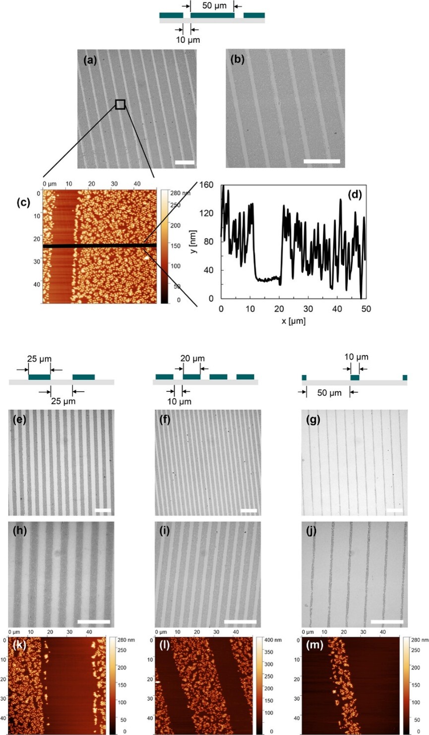
Atomic force microscopy (AFM) was employed to characterize the morphology and surface structure of the synthesized microgels after deposition. High-resolution AFM imaging was performed in tapping mode using a NanoWorld PointProbe® NCH AFM probe. The silicon AFM probe, featuring a resonance frequency of approximately 320 kHz and a spring constant of 42 N/m, enabled detailed visualization of the microgel topography and provided valuable information on particle morphology and surface organization at the nanoscale.
AFM characterization complemented dynamic light scattering and zeta potential measurements by providing direct nanoscale imaging of the surface-coated microgels. The high spatial resolution of the NanoWorld PointProbe® NCH AFM probe allowed the authors to verify the successful formation of uniform microgel structures, supporting the optimization of the microcontact printing process and the subsequent surface functionalization steps.
This article demonstrates how NanoWorld AFM probes contribute to the characterization of advanced polymeric microgel systems used for surface engineering. By combining high-resolution AFM imaging with microcontact printing and post-functionalization strategies, the study provides new opportunities for designing multifunctional surfaces for biomedical, biotechnology, and materials science applications.
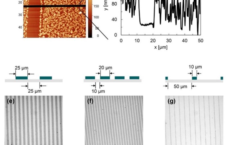
Figure 3 Imaging of surfaces structured with p(VCL-co-10mol%GMA-shell) microgels via microcontact printing. a,b,e-j) Light microscopy images and c,k-m) AFM images were recorded. Additionally, d) shows a height profile generated from the AFM image b). The ideal dimensions of resulting patterns are given in the schemes above. Dark grey areas in light microscopy images represent microgel stripes, lighter areas represent the bare glass. Scale bars in light microscopy images: 100 µm.
Full citation:
Litzen, I.; Töpel, A.; Zenke, M.; Sechi, A.; Pich, A. Multifunctional Microstructured Surfaces by Microcontact Printing of Reactive Microgels. Advanced Functional Materials36(15), e16135 (2026). https://doi.org/10.1002/adfm.202516135
A reliable replacement of the Olympus®* AC160 –
Optimized Positioning with Maximum AFM Tip Visibility
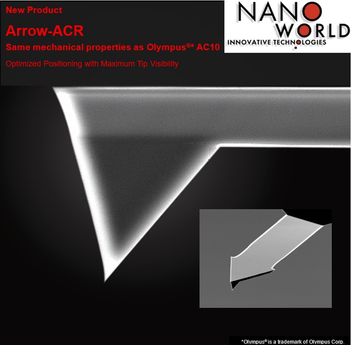
NanoWorld AG is pleased to introduce the new Arrow-ACR AFM probe, developed to provide research professionals worldwide with a dependable alternative to the discontinued Olympus®* AC160 microcantilever.
The Arrow™ ACR (typical resonance frequency 300 kHz, typical force constant 26 N/m), combines identical mechanical properties as the
Olympus®* AC160 with the well-known Arrow AFM tip and cantilever geometry. Always positioned exactly at the end of the AFM cantilever, this AFM probe offers easy positioning of the AFM tip over the area of interest.
With their moderate stiffness (typical force constant 26 N/m) the Arrow™ ACR probes are particularly suitable for studying relatively soft materials, including various polymers. These AFM probes are designed to perform optimally in non-contact/Tapping™ mode in air, enabling detailed characterization of thin films, coatings, surface roughness, and localized defects.
Users can expect stable operation, high sensitivity and high-speed scanning capabilities, ensuring reproducible data across a wide range of applications.
For researchers seeking a seamless transition from the discontinued
Olympus®* AC160, the NanoWorld® Arrow™ ACR offers a reliable solution backed by NanoWorld’s manufacturing precision and quality control.
A reliable replacement of the Olympus®* AC160 – NanoWorld introduces new Arrow-ACR Silicon AFM probe Optimized Positioning with Maximum AFM Tip Visibility
Flux-closure structures, vortices/antivortices, skyrmions, and merons in oxides, metals and polymers represent non-trivial topologies in which a local polar/magnetic order undergoes quasi-continuous spatial variations in a host crystal lattice. These structures are now extensively studied due to emergent functionalities, but the application of electrical/mechanical fields has so far only served to destroy the polar topologies of interest. *
Topology created by quasi-continuous spatial variations of a local polarization direction represents an exotic state of matter, but field-driven manipulation has been hitherto limited to creation and destruction. *In the article “Electrically and mechanically driven rotation of polar spirals in a relaxor ferroelectric polymer” Mengfan Guo, Erxiang Xu, Houbing Huang, Changqing Guo, Hetian Chen, Shulin Chen, Shan He, Le Zhou, Jing Ma, Zhonghui Shen, Ben Xu, Di Yi, Peng Gao, Ce-Wen Nan, Neil. D. Mathur and Yang Shen report that relatively small electric or mechanical fields can drive the non-volatile rotation of polar spirals in discretized microregions of the relaxor ferroelectric polymer poly(vinylidene fluoride-ran-trifluoroethylene).*
These polar spirals arise from the asymmetric Coulomb interaction between vertically aligned helical polymer chains, and can be rotated in-plane through various angles with robust retention. *
Given also that their manipulation of topological order can be detected via infrared absorption, Mengfan Guo et al.’s work suggests a new direction for the application of complex materials. *
Mengfan Guo et al. produced a 100-nm-thick monolayer of face-on lamellae with vertically aligned polymer chains by melt-recrystallizing spin-coated thin films of P(VDF-TrFE).
The resulting melt-recrystallized thin film of the relaxor ferroelectric polymer was characterized by the authors using a commercial atomic force microscope for in-plane piezo-response force microscopy (IP-PFM).
NanoWorld Platinum Iridium coated Arrow-CONTPt AFM probes (typical resonant frequency: 14 kHz, typical force constant: 0.2 N/m, typical AFM tip radius 25 nm) were used for the in-plane (IP) PFM tests and the PFM lithography tests.
For piezo-response force microscopy (PFM) imaging, Vector mode was used where AFM tips were modulated at around 240 kHz for IP imaging, with the AC voltage set at 2 V. The images obtained by Vector Mode were double checked by using dual AC resonance tracking (DART) mode and the patterns could be reproduced. *
For angle-resolved IP-PFM tests, the rotation of sample was controlled by a protractor. To ensure identical position was imaged after rotating the sample, the authors made cross-scratches as a mark on the sample surface in advance. This method was applied to locate the scanning position in other situations if Mengfan Guo et al. had to move the sample in between the scanning probe microscopic studies.
For electric-field-induced manipulations using PFM lithography, the DC voltage on AFM tip was previously edited in the software. The scan speed was set at 1.95 Hz and no AC voltage was applied during the scanning. The DC voltage was divided by film thickness (100 nm) to obtain the electric field value. And an electric field with downward direction is defined with a positive sign.
For stress-induced manipulations, the deflection value of the PFM cantilever, which is a signal from photodetector, was preset to control the stress/force applied onto the sample. The difference in deflection value between a pressed AFM cantilever and a free AFM cantilever reflects how hard the AFM tip and sample surface are pressed to each other.*
To obtain the force value F, Mengfan Guo et al. first calibrated the AFM tips by the thermal noise method, and obtain the inverse optical lever sensitivity (InvOLS) and the spring constant k of the AFM tips.
The authors also conducted a polarization analysis based on their PFM measurements. *
To obtain the nominal toroidal order evaluated by the local curvature, the obtained IP-PFM amplitude image was firstly divided into 33 × 33 arrays, and each region was then subjected to a recognition of potential domain walls and measurement of an averaged curvature radius. *
To obtain polarization maps, angle-resolved IP-PFM images were first aligned to correct spatial distortion in nanoscale measurement. Positions with specific morphological characteristics were selected as reference points to determine the coordinate. After the correction, improved angle-resolved IP-PFM phase images would be divided into 64 × 64 arrays for deriving polarization maps. *
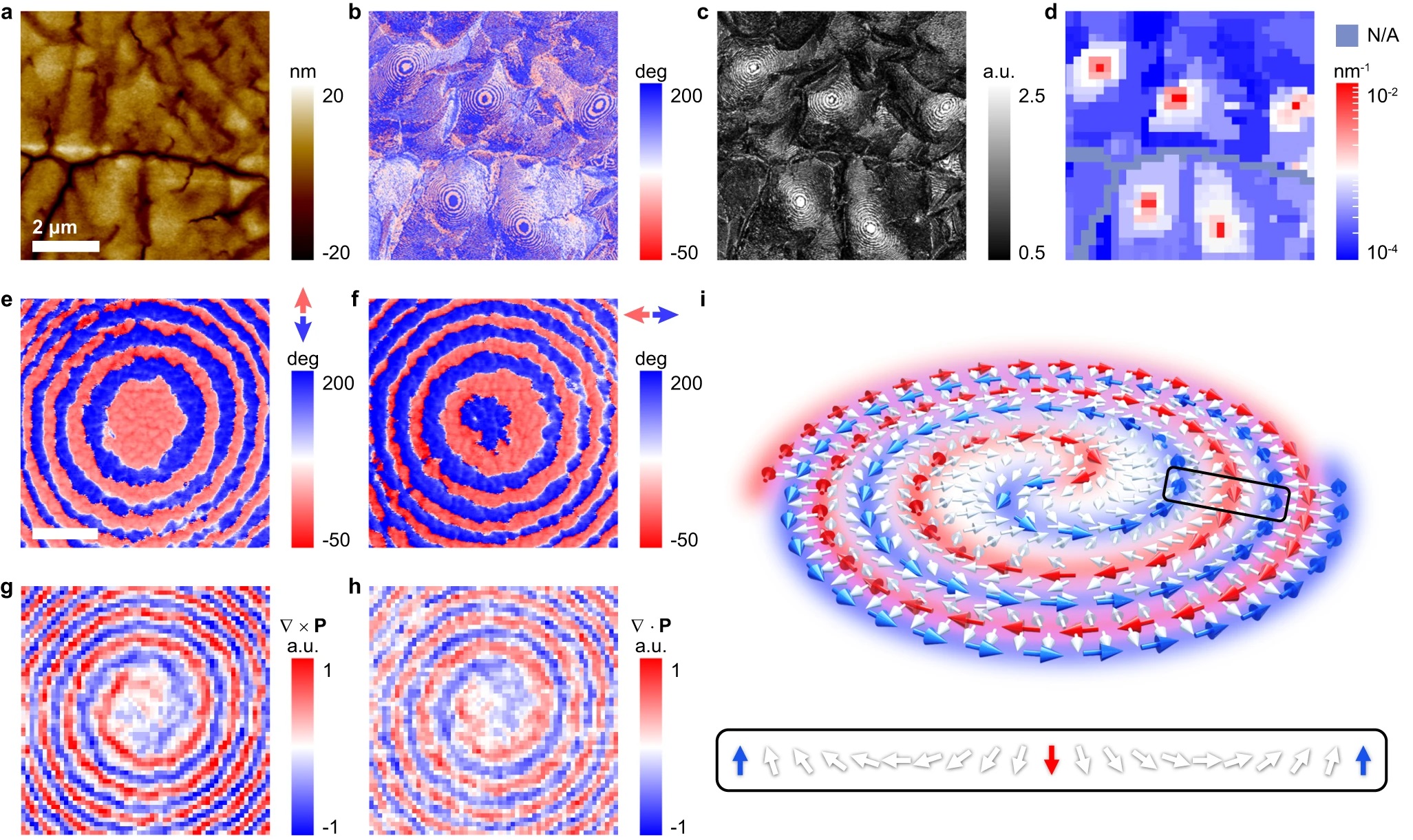
Fig. 1 from Mengfan Guo et al. (2024) “Electrically and mechanically driven rotation of polar spirals in a relaxor ferroelectric polymer”: Observation of a microregion containing an in-plane polar spiral. a Morphology of a melt-recrystallized thin film of the relaxor ferroelectric polymer. The scale bar is 2 μm. IP-PFM phase (b) and amplitude (c) images of the same area in a exhibiting concentric ring-shaped domains in curly stripe domains. d Distribution of domain wall curvatures in the same area in a–c evidencing nominal toroidal order. It is assumed that the local polarization is parallel to the nearest domain wall so that larger curvature (denoted red) reflects stronger toroidal order. IP-PFM phase images of identical concentric ring-shaped domains with the axis along vertical (e) and horizontal (f) measurement directions. The scale bar is 0.3 μm. The curl (g) and the divergence (h) of local polarization in the same area as e and f, revealing the polar spiral topology. i Schematic stereoscopic view of a CCW polar spiral, arrows represent regions of polarization. The red/blue arrows denote the polar source/sink that spirals in/out. The white arrows represent Néel rotation along the radial direction, as shown in more detail via the inset.
*Mengfan Guo, Erxiang Xu, Houbing Huang, Changqing Guo, Hetian Chen, Shulin Chen, Shan He, Le Zhou, Jing Ma, Zhonghui Shen, Ben Xu, Di Yi, Peng Gao, Ce-Wen Nan, Neil. D. Mathur and Yang Shen Electrically and mechanically driven rotation of polar spirals in a relaxor ferroelectric polymer
Nature Communications volume 15, Article number: 348 (2024)
DOI: https://doi.org/10.1038/s41467-023-44395-5
The article “Electrically and mechanically driven rotation of polar spirals in a relaxor ferroelectric polymer” by Mengfan Guo, Erxiang Xu, Houbing Huang, Changqing Guo, Hetian Chen, Shulin Chen, Shan He, Le Zhou, Jing Ma, Zhonghui Shen, Ben Xu, Di Yi, Peng Gao, Ce-Wen Nan, Neil. D. Mathur and Yang Shen is licensed under a Creative Commons Attribution 4.0 International License, which permits use, sharing, adaptation, distribution and reproduction in any medium or format, as long as you give appropriate credit to the original author(s) and the source, provide a link to the Creative Commons license, and indicate if changes were made. The images or other third-party material in this article are included in the article’s Creative Commons license, unless indicated otherwise in a credit line to the material. If material is not included in the article’s Creative Commons license and your intended use is not permitted by statutory regulation or exceeds the permitted use, you will need to obtain permission directly from the copyright holder. To view a copy of this license, visit https://creativecommons.org/licenses/by/4.0/.