Piezoelectricity of green carp scales

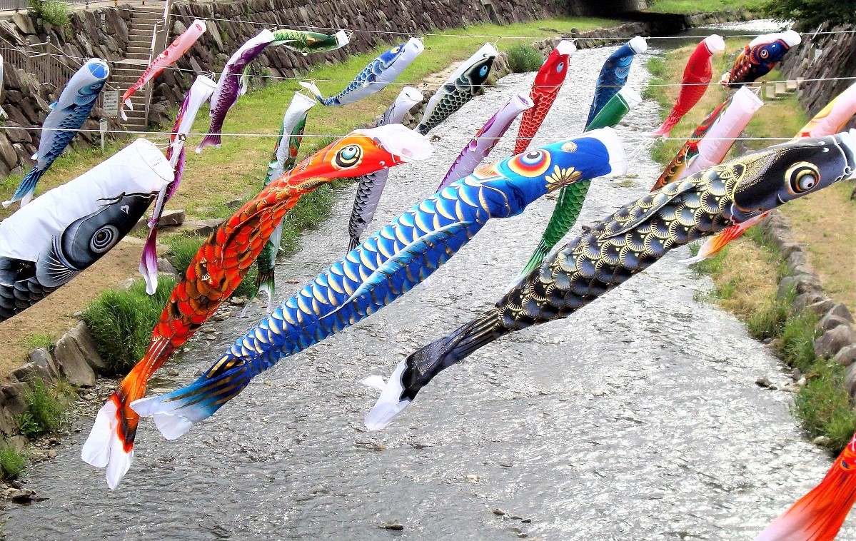
Today is Children’s Day in Japan and many mulit-colored carp-shaped koinobori streamers are fluttering in the wind.

So it is the perfect day to repost and share the publication “Piezoelectricity of green carp scales” by Y. Jiang et al. with you.

Piezoelectricity takes part in multiple important functions and processes in biomaterials often vital to the survival of organisms. In their publication , “Piezoelectricity of green carp scales” Y. Jiang et al. investigate the piezoelectric properties of fish scales of green carp by directly examining their morphology at nanometer levels. From the clear distinctions between the composition of the inner and outer surfaces of the scales that could be found, the authors identified the piezoelectricity to originate from the presence of hydroxyapatite which only exists on the surface of the fish scales.*

koinobori - carp streamers on children's day in Matsumoto Japan
koinobori – carp streamers on children’s day in Matsumoto Japan

These findings reveal a different mechanism of how green carp are sensitive to their surroundings and should be helpful to studies related to the electromechanical properties of marine life and the development of bio-inspired materials. As easily accessible natural polymers, fish scales can be employed as highly sensitive piezoelectric materials in high sensitive and high speed devices as well as be exploited for invasive diagnostics and other biomedical implications.*

For the harmonic responses of both 1st order and 2nd order described in this publication, NanoWorld Arrow-CONTPt AFM probes were used.

FIG. 6 from “Piezoelectricity of green carp scales “ by H. Y. Jiang et al.: First and second harmonic responses of (a) domain I and (b) domain IV. The straight line fitting for the amplitude of first harmonic response of (c) domain I and (d) domain IV by applying a series of bias. NanoWorld Arrow-CONTPt AFM probes were used.
FIG. 6 from “Piezoelectricity of green carp scales “ by H. Y. Jiang et al.: First and second harmonic responses of (a) domain I and (b) domain IV. The straight line fitting for the amplitude of first harmonic response of (c) domain I and (d) domain IV by applying a series of bias.

*Y. Jiang, F. Yen, C. W. Huang, R. B. Mei, and L. Chen
Piezoelectricity of green carp scales
AIP Advances 7, 045215 (2017)
DOI: https://doi.org/10.1063/1.4979503

Please follow this external link to access the full article: https://aip.scitation.org/doi/full/10.1063/1.4979503

Open Access The article “Piezoelectricity of green carp scales” by Y. Jiang, F. Yen, C. W. Huang, R. B. Mei and L. Chen is licensed under a Creative Commons Attribution 4.0 International License, which permits use, sharing, adaptation, distribution and reproduction in any medium or format, as long as you give appropriate credit to the original author(s) and the source, provide a link to the Creative Commons license, and indicate if changes were made. The images or other third party material in this article are included in the article’s Creative Commons license, unless indicated otherwise in a credit line to the material. If material is not included in the article’s Creative Commons license and your intended use is not permitted by statutory regulation or exceeds the permitted use, you will need to obtain permission directly from the copyright holder. To view a copy of this license, visit http://creativecommons.org/licenses/by/4.0/.



Optimized positioning through maximized tip visibility – Arrow AFM probes screencast passes 500 views mark

The screencast about NanoWorld Arrow Silicon AFM probes held byNanoWorld AG CEO Manfred Detterbeck has just passed the 500 views mark. Congratulations Manfred!

NanoWorld Arrow™ AFM probes are designed for easy AFM tip positioning and high resolution AFM imaging and are very popular with AFM users due to the highly symetric scans that are possible with these AFM probes because of their special tip shape. They fit to all well-known commercial SPMs (Scanning Probe Microscopes) and AFMs (Atomic Force Microscopes). The Arrow AFM probe consists of an AFM probe support chip with an AFM cantilever which has a tetrahedral AFM tip at its triangular free end.

The Arrow AFM probe is entirely made of monolithic, highly doped silicon.

The unique Arrow™ shape of the AFM cantilever with the AFM tip always placed at the very end of the AFM cantilever allows easy positioning of the AFM tip on the area of interest.
The Arrow AFM probes are available for non-contact mode, contact mode and force modulation mode imaging and are also available with a conductive platinum iridum coating. Furthermore the Arrow™ AFM probe series also includes a range of tipless AFM cantilevers and AFM cantilever arrays as well as dedicated ultra-high frequency Arrow AFM probes for high speed AFM.

To find out more about the different variations please have a look at:

https://www.nanoworld.com/arrow-afm-tips

You can also find various application examples for the Arrow AFM probes in the NanoWorld blog. For a selection of these articles just click on the “Arrow AFM probes” tag on the bottom of this blog entry.


Quantification of electron accumulation at grain boundaries in perovskite polycrystalline films by correlative infrared-spectroscopic nanoimaging and Kelvin probe force microscopy

Organic-inorganic halide perovskites are materials of high interest for the development of solar cells.

Learning more about the relationship between the electrical properties and the chemical compositions of perovskite at the nanoscale can help to understand how the interrelations of both can affect device performance and contribute to an understanding on how to best design perovskite active layer structures.*

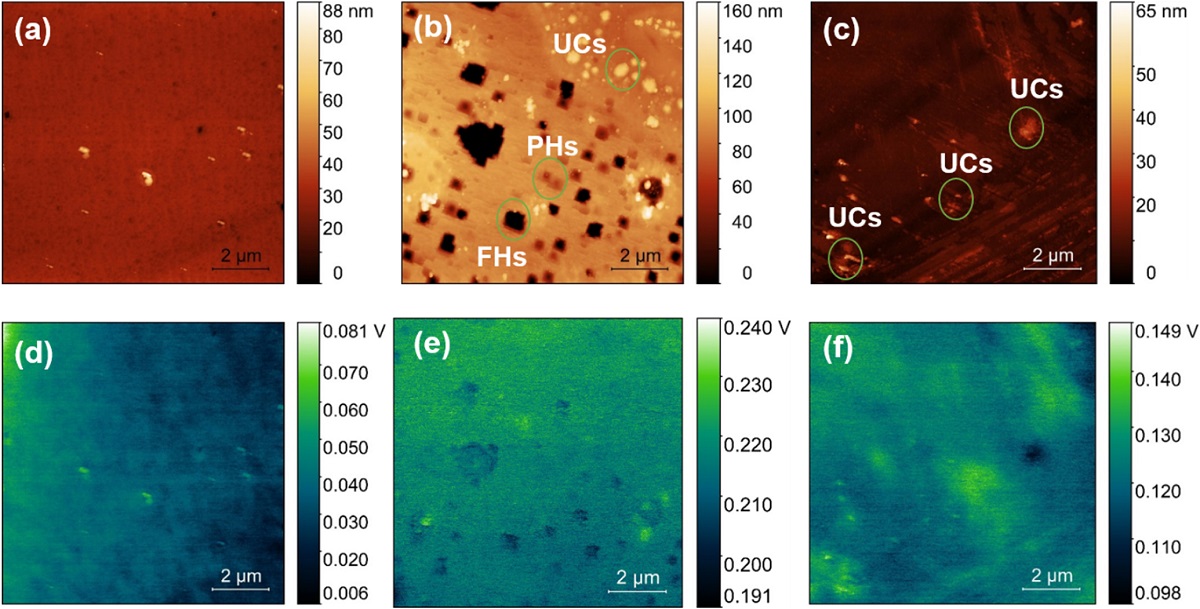
For the article “Quantification of electron accumulation at grain boundaries in perovskite polycrystalline films by correlative infrared-spectroscopic nanoimaging and Kelvin probe force microscopy” Ting-Xiao Qin, En-Ming You, Mao-Xin Zhang, Peng Zheng, Xiao-Feng Huang, Song-Yuan Ding, Bing-Wei Mao and Zhong-Qun Tian used correlative infrared-spectroscopic nanoimaging ( IR-spectroscopy ) by scattering-type scanning near-field optical microscopy ( s-SNOM ) and Kelvin probe force microscopy ( KPFM ) to contribute to the discussion whether nanometer-sized grain boundaries (GBs) in polycrystalline perovskite films play a positive or negative role in solar cell performance.*

The integrated KPFM and s-SNOM measurements were performed by the authors to acquire the surface potential and infrared near-field image simultaneously through a single-pass scan and thereby learn more about the relationships between the electrical properties and spectral information at the grain boundaries of the investigated material ( polycrystalline CH3NH3Pbl3 perovskite films ).*

The results of the correlated s-SNOM and KPFM imaging presented in the article show that the electron accumulations are enhanced at the grain boundaries (GBs) of the investigated polycrystalline perovskite film, particularly under light illumination which would assist in electron-hole separation and therefore would be a positive influence on the performance of the solar cell.*

NanoWorld conductive platinum-iridium coated Arrow AFM probes ( Arrow-NCPt ) were used to perform the s-SNOM IR imaging.

Figure 4 from “Quantification of electron accumulation at grain boundaries in perovskite polycrystalline films by correlative infrared-spectroscopic nanoimaging and Kelvin probe force microscopy” by Ting-Xiao Qin  et al.
Correlative KPFM and s-SNOM nanoimaging on perovskite.
a AFM topography (1 μm × 1 μm); b Contact potential difference (CPD); and c simultaneously acquired infrared near-field image; d one-dimensional line profiles of the topography, CPD and infrared near-field amplitude along the white dashed lines marked in a–c. The scale bars are 200 nm.
NanoWorld Arrow-NCPt AFM probes were used to perform the s-SNOM IR imaging
Figure 4 from “Quantification of electron accumulation at grain boundaries in perovskite polycrystalline films by correlative infrared-spectroscopic nanoimaging and Kelvin probe force microscopy” by Ting-Xiao Qin  et al.
Correlative KPFM and s-SNOM nanoimaging on perovskite.
a AFM topography (1 μm × 1 μm); b Contact potential difference (CPD); and c simultaneously acquired infrared near-field image; d one-dimensional line profiles of the topography, CPD and infrared near-field amplitude along the white dashed lines marked in a–c. The scale bars are 200 nm.

*Ting-Xiao Qin, En-Ming You, Mao-Xin Zhang, Peng Zheng, Xiao-Feng Huang, Song-Yuan Ding, Bing-Wei Mao and Zhong-Qun Tian
Quantification of electron accumulation at grain boundaries in perovskite polycrystalline films by correlative infrared-spectroscopic nanoimaging and Kelvin probe force microscopy
Light: Science & Applications volume 10, Article number: 84 (2021)
DOI: https://doi.org/10.1038/s41377-021-00524-7

Please follow the external link to read the whole article: https://rdcu.be/clg7f

Open Access : The article “Quantification of electron accumulation at grain boundaries in perovskite polycrystalline films by correlative infrared-spectroscopic nanoimaging and Kelvin probe force microscopy” by Ting-Xiao Qin, En-Ming You, Mao-Xin Zhang, Peng Zheng, Xiao-Feng Huang, Song-Yuan Ding, Bing-Wei Mao and Zhong-Qun Tian is licensed under a Creative Commons Attribution 4.0 International License, which permits use, sharing, adaptation, distribution and reproduction in any medium or format, as long as you give appropriate credit to the original author(s) and the source, provide a link to the Creative Commons license, and indicate if changes were made. The images or other third party material in this article are included in the article’s Creative Commons license, unless indicated otherwise in a credit line to the material. If material is not included in the article’s Creative Commons license and your intended use is not permitted by statutory regulation or exceeds the permitted use, you will need to obtain permission directly from the copyright holder. To view a copy of this license, visit https://creativecommons.org/licenses/by/4.0/.