Hydrogel materials show a number of properties which make them interesting candidates to be utilized to mimic the extracellular matrix (ECM). Therefore, these materials are attractive for use in biological applications such as tissue engineering, cell culture 3D bioprinting and more.
Are you planning to use hydrogels for the first time in your research?
Then have a look at the insightful article “A beginner’s guide to the Characterization of Hydrogel Microarchitecture for Cellular Applications” by Francisco Drusso Martinez-Garcia, Tony Fischer, Alexander Hayn, Claudia Tanja Mierke, Janette Kay Burgess and Martin Conrad Harmsen.
In their article the authors describe and evaluate the different technologies that are most commonly used to assess hydrogel microarchitecture.
Francisco Drusso Martinez-Garcia et al. explain the working principle of the various methods and also discuss the merits and limitations of each of them in view of their usefulness for the characterization of hydrogels.
They introduce and explore the pros and cons of the following methods: Scanning Electron Microscopy (SEM), Cryogenic Scanning Electron Microscopy (Cryo-SEM), Environmental Scanning Electron Microscopy (ESEM), Micro-Computed Tomography (µ-CT), Confocal Laser Scanning Microscopy (CLSM), Second Harmonic Generation and Atomic Force Microscopy (AFM).*
Atomic force microscopy (AFM) can be used to investigate the hydrogel surface topology as well as a hydrogel’s mechanical properties. The latter can be achieved through mathematical modelling of force-distance curves.
When using the AFM to characterize the elasticity of a hydrogel sample it is essential to take the stiffness of the investigated material into account when choosing what kind of AFM probe to use for these experiments.
If an AFM cantilever used for probing a soft sample is too stiff (if the force constant/spring constant is too high) this might result in a poor signal-to-noise ratio.
If a soft AFM probe (an AFM probe with an AFM cantilever with a low force constant) is chosen to investigate a soft material this should lead to a better signal-to-noise ratio. On the other hand, if an AFM cantilever is too soft (if the force constant is too low) then it might not be stiff enough to indent the investigated material.
Another critical factor is the shape and the size of the AFM tip.
Spheroidal AFM probes might stick to the material, resulting in artefacts, disrupted force–distance curves, or even damaged AFM cantilevers. If the AFM tip is much smaller than the pore size of the hydrogel, it might get stuck in the fibrous network microarchitecture.
On the other hand, if the spherical AFM tip, e.g. as in colloidal AFM probes (a sphere glued to end of a tipless AFM cantilever), is too large, the weight of the sphere can have a negative influence on the spring characteristics of the AFM cantilever.
All these factors and more as described in the cited article have to be carefully weighed before deciding on the settings of the atomic force microscope and choosing an AFM probe for the investigation of a specific hydrogel.
NanoWorld tipless ArrowTL2 cantilever arrays with polystyrene beads glued to them were used by the authors of this beginner’s guide to achieve the AFM data presented in the article.*
Figure 6. from Francisco Drusso Martinez-Garcia et al. 2022: Atomic force microscopy. (A) Equipment. (B) Schematic of an AFM setup with a four-quadrant photodiode (1), in which the four-quadrant photodiode (1) receives a laser (2) reflected from a cantilever (3), in this case positioned over a hydrogel (4) mounted in a piezo stage (5). For example, the height differences in a sample (4) are measured by adjusting the stage using piezo elements (5) to counter the cantilever bending on a nanometer scale. (C) The AFM can then generate a surface heightmap of the hydrogels such as a GelMA hydrogel (shown). AFM can also be used to determine the mechanical properties of hydrogels. (D) Schematic of the AFM technique to determine the elastic moduli of hydrogels with a tipless cantilever (1), spheroidal probe (2, red), hydrogel (3), and stiff substrate (4). As the cantilever represents a spring with a known spring constant, the cantilever bending due to elastic counterforces exerted by the soft material is correlated with the piezo stage height (4). (E) The so-called force–distance curves are recorded. Data from a collagen type-I hydrogel (3.0 g/L) are shown. (F) Young’s moduli of a 1.5 g/L and 3.0 g/L collagen type-I hydrogel. Outliers indicated by ◆. AFM equipment detailed in Appendix A of the cited article.
NanoWorld® Arrow™ TL2 AFM probes are tipless AFM cantilevers for special applications. They can for example be used for attaching spheres and other objects to the free end of the AFM cantilever, or for functionalizing and sensing applications. The Arrow™ TL2 probes are optionally available with a sample facing side gold coating (Arrow™ TL2Au).
*Francisco Drusso Martinez-Garcia, Tony Fischer, Alexander Hayn, Claudia Tanja Mierke, Janette Kay Burgess and Martin Conrad Harmsen A Beginner’s Guide to the Characterization of Hydrogel Microarchitecture for Cellular Applications Gels 2022, 8(9), 535
DOI: https://doi.org/10.3390/gels8090535
The article “A Beginner’s Guide to the Characterization of Hydrogel Microarchitecture for Cellular Applications” by Francisco Drusso Martinez-Garcia, Tony Fischer, Alexander Hayn, Claudia Tanja Mierke, Janette Kay Burgess and Martin Conrad Harmsen is licensed under a Creative Commons Attribution 4.0 International License, which permits use, sharing, adaptation, distribution and reproduction in any medium or format, as long as you give appropriate credit to the original author(s) and the source, provide a link to the Creative Commons license, and indicate if changes were made. The images or other third-party material in this article are included in the article’s Creative Commons license, unless indicated otherwise in a credit line to the material. If material is not included in the article’s Creative Commons license and your intended use is not permitted by statutory regulation or exceeds the permitted use, you will need to obtain permission directly from the copyright holder. To view a copy of this license, visit https://creativecommons.org/licenses/by/4.0/.
The products of the polyurethane (PU) industry such as foams, coatings and adhesives are numerous and can be found in many areas of everyday life. *
Polyols are an essential component in the production of polyurethane. Nowadays they mostly come from petroleum products. *
In view of potential risk factors such as the running out of fossil fuels, supply chain issues, environmental concerns and economic risks it is important to develop alternatives as substitutes and supplements to the existing petroleum derived polyols. *
Vegetable oils can be used to manufacture biobased polyols and various oils such as linseed oil, rapeseed oil, canola oil, grapeseed oil, corn oil, rice bran oil, palm oil, olive oil, castor oil and soybean oil have already been used to make polyols for different purposes.*
Most of the polyols derived from vegetable oils that are already commercially available are made from soybean and castor oil and are mainly used for rigid PU foam applications. *
So far biobased materials for flexible polyurethane foams (FPUFs) have not been studied as much as their rigid counterpart. This is because, due to their chemical composition, there are limits to how much biobased materials can be used in the flexible foam without having an undesired effect on the foam’s mechanical properties. *
Coconut oil is not often used to manufacture flexible foam because the coconut oil’s high level of saturation makes it less compatible with many common methods of creating polyols, as the widely used polyol-forming processes mostly rely on the unsaturation of vegetable oil for functionalization.
To make coconut monoglycerides (CMG) or other plant-based oils usable for polyol-forming processes they need to fulfil the same structural requirements as the fossil-based products. *
In the article “Flexible Polyurethane Foams Modified with Novel Coconut Monoglycerides-Based Polyester Polyols “ Christine Joy M. Omisol, Blessy Joy M. Aguinid, Gerson Y. Abilay, Dan Michael Asequia, Tomas Ralph Tomon, Karyl Xyrra Sabulbero, Daisy Jane Erjeno, Carlo Kurt Osorio, Shashwa Usop, Roberto Malaluan, Gerard Dumancas, Eleazer P. Resurreccion, Alona Lubguban, Glenn Apostol, Henry Siy, Arnold C. Alguno, and Arnold Lubguban describe how they investigated the potential of coconut monoglycerides (CMG) as a polyol raw material specifically for flexible polyurethane foam (FPUF) applications.*
The authors synthesized high-molecular-weight polyester polyols from coconut monoglycerides (CMG), a coproduct of fatty acid production from coconut oil, via polycondensation at different mass ratios of CMG with 1:5 glycerol:phthalic anhydride.*
The resulting CMG-based polyols were shown to work well in making flexible foam. *
Fourier transform infrared (FTIR) spectroscopy and atomic force microscopy (AFM) were used for the foam characterization. *
The modification of the foam formulation increased the monodentate and bidentate urea groups, shown using Fourier transform infrared (FTIR) spectroscopy, that promoted microphase separation in the foam matrix, confirmed using atomic force microscopy (AFM) and differential scanning calorimetry (DSC). *
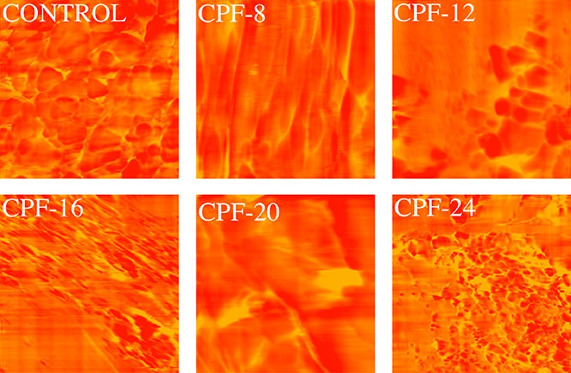
Atomic force microscopy (AFM) was used to evaluate the hard–soft domains phase separation of the foam. *
The atomic force microscope was operated at a scan rate of 1.0 Hz in non-contact mode using NanoWorld Pointprobe®NCHR Silicon AFM probes for standard tapping mode applications. (typical resonance frequency 320 kHz, typical force constant 42 N/m). *
It could be shown that density of the CMGPOL-modified polyurethane foams (CPFs) decreased, while a significant improvement in their tensile and compressive properties was observed. *
The investigations by Christine Joy M. Omisol et al. resulted in a new sustainable polyol raw material that can be used to modify petroleum-based foam and produce flexible foams with varying properties that can be tailored to meet specific requirements. *
Figure 11 from Christine Joy M. Omisol et al (2024) “Flexible Polyurethane Foams Modified with Novel Coconut Monoglycerides-Based Polyester Polyols”: Atomic force microscopy (AFM) phase images of CMGPOL-modified polyurethane foams (CPF) and control foam measured with a size scan of 3 μm × 3 μm showing soft and hard regions represented by red and yellow colors, respectively.
*Christine Joy M. Omisol, Blessy Joy M. Aguinid, Gerson Y. Abilay, Dan Michael Asequia, Tomas Ralph Tomon, Karyl Xyrra Sabulbero, Daisy Jane Erjeno, Carlo Kurt Osorio, Shashwa Usop, Roberto Malaluan, Gerard Dumancas, Eleazer P. Resurreccion, Alona Lubguban, Glenn Apostol, Henry Siy, Arnold C. Alguno, and Arnold Lubguban Flexible Polyurethane Foams Modified with Novel Coconut Monoglycerides-Based Polyester Polyols
ACS Omega 2024, 9, 4, 4497–4512
DOI: https://doi.org/10.1021/acsomega.3c07312
The article “Flexible Polyurethane Foams Modified with Novel Coconut Monoglycerides-Based Polyester Polyols” by Christine Joy M. Omisol, Blessy Joy M. Aguinid, Gerson Y. Abilay, Dan Michael Asequia, Tomas Ralph Tomon, Karyl Xyrra Sabulbero, Daisy Jane Erjeno, Carlo Kurt Osorio, Shashwa Usop, Roberto Malaluan, Gerard Dumancas, Eleazer P. Resurreccion, Alona Lubguban, Glenn Apostol, Henry Siy, Arnold C. Alguno and Arnold Lubguban is licensed under a Creative Commons Attribution 4.0 International License, which permits use, sharing, adaptation, distribution and reproduction in any medium or format, as long as you give appropriate credit to the original author(s) and the source, provide a link to the Creative Commons license, and indicate if changes were made. The images or other third-party material in this article are included in the article’s Creative Commons license, unless indicated otherwise in a credit line to the material. If material is not included in the article’s Creative Commons license and your intended use is not permitted by statutory regulation or exceeds the permitted use, you will need to obtain permission directly from the copyright holder. To view a copy of this license, visit https://creativecommons.org/licenses/by/4.0/.