Known as a rising star among carbon nanomaterials, carbon dots (CDs) have attracted considerable interest in various fields in recent years.*
In the article “Highly efficient carbon dot-based photoinitiating systems for 3D-VAT printing” Dominika Krok, Wiktoria Tomal, Alexander J. Knight, Alexander I. Tartakovskii, Nicholas T. H. Farr, Wiktor Kasprzyk and Joanna Ortyl describe how they synthesized different types of carbon dots (CDs) based on citric acid as a precursor using an efficient procedure to purify these materials from low molecular by-products and fluorophores.*
They introduce three types of CDs: citric acid-based, as well as ammonia- and ethylenediamine-doped CDs, and compare their effectiveness to commercially available graphene-based CDs as an element of two- or three-component photoinitiating systems dedicated for free radical photopolymerization processes.*
This approach led to the development of efficient initiating systems and allowed better understanding of the mechanism according to which CDs performed in these processes. *
As the proof of concept, CDs-based photoinitiating systems were implemented in two types of 3D-VAT printing processes: DLP and DLW printing, to obtain high-resolution, 3D hydrogel materials. *
Dominika Krok et al. believe that the research presented in their article will become the basis for further work on carbon dots in the context of the diverse use of photopolymerization processes and avoid errors affecting the misinterpretation of data. *
The morphology and chemical composition of obtained hydrogel printouts were profoundly characterized via scanning electron microscopy (SEM), atomic force microscopy (AFM), nanoscale Fourier transform infrared spectroscopy (Nano-FTIR), and scattering-type Scanning Near-field Optical Microscopy (s-SNOM). *
The s-SNOM system used to collect the data shown in figure 12 of the article cited below, consisted of an AFM within one arm of an interferometer, and a moveable mirror in the other. *
A conductive platinum-iridium coated NanoWorld ARROW-EFM AFM probe was brought into tapping mode operation upon the sample (tapping frequency 77 kHz, tapping amplitude 71 nm), and illumination from a single-wavelength source outputting at 1490 cm−1 was sent into the interferometer. *
Under focused illumination, the conductive AFM tip acts as an optical antenna and a near field is generated at the AFM tip apex (AFM tip radius around 25 nm). The near field interacts with the sample surface and forms a scattering centre that scatters further incoming photons. *
The scattered photons were collected at the detector and interfered with photons returning from the movable mirror in the reference arm of the interferometer. This reference mirror was oscillated in order to induce side-band frequency mixing in the optical signal power spectrum, and the optical amplitude and phase data were extracted at the third harmonic of the AFM tapping frequency. *
The optical amplitude data were normalised to the maximum recorded value. The optical phase data were left unprocessed, and thus the raw values of the phase data in Fig. 12 (cited below) do not hold physical meaning. Only the contrast between two areas of Fig. 12 should be considered. *
AFM data: AFM topology data were recorded using the same instrument as used for the s-SNOM measurements. Conductive AFM cantilevers (Pt/Ir coated ARROW-EFM AFM probes from NanoWorld) were used, at a tapping frequency of 77 kHz and a tapping amplitude of 71 nm. *
Further surface characterization of the hydrogel samples performed with AFM and s-SNOM techniques revealed that, occasionally, carbon dot particles can be found at or emerging from the surface of the hydrogel. *
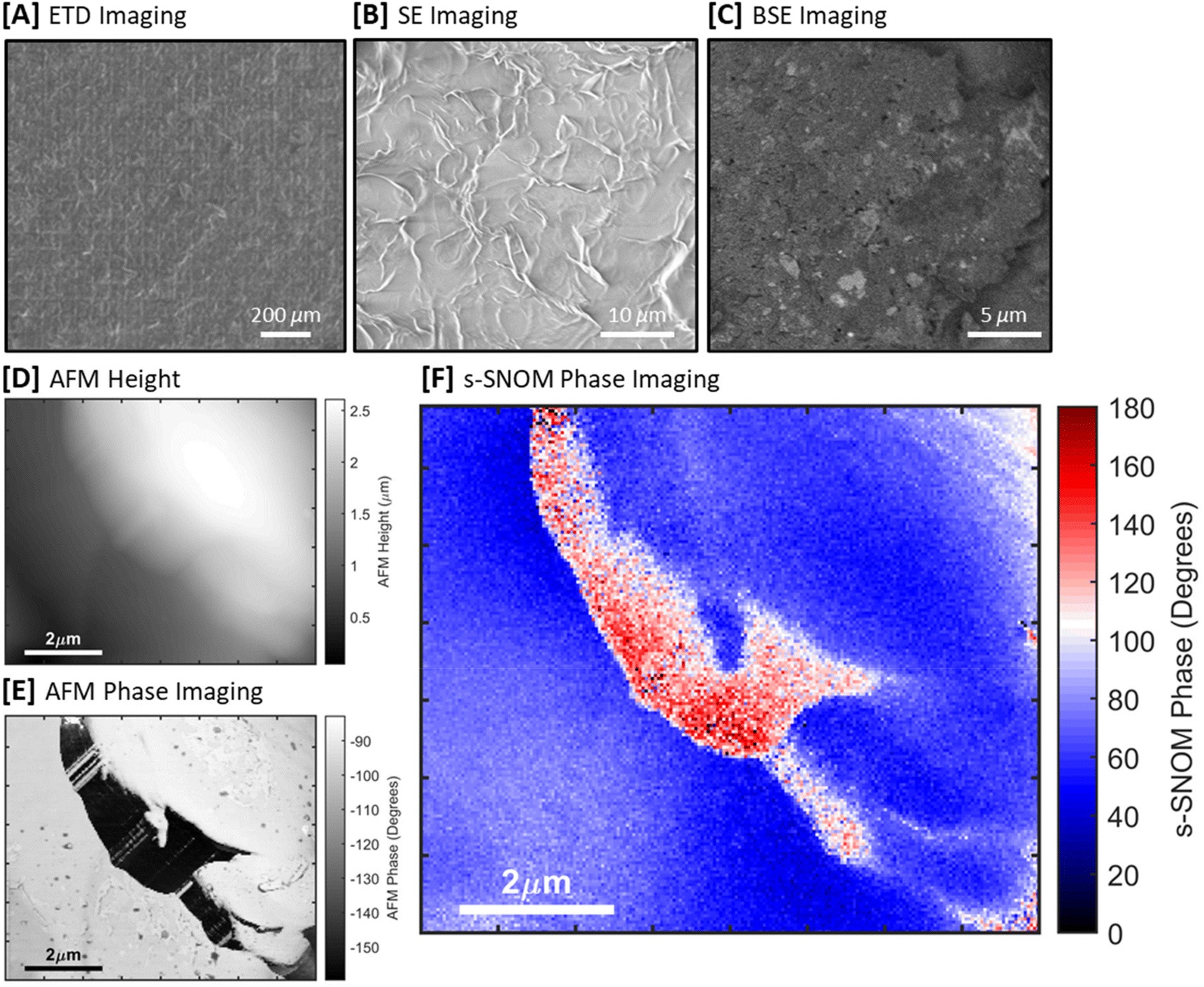
Fig. 12D presents the surface topography of an 8 μm by 6.8 μm region of hydrogel as measured through AFM, which is in keeping with the surface characterization data presented in Fig. 12A–C. It is not obvious from the topography data in Fig. 12D alone which features of the sample surface relate to carbon material. *
However, the carbon dot particles can be identified through the mechanical properties of their surface: Fig. 15E in the cited article presents the AFM phase data from the scan shown in Fig. 12D, with AFM phase being sensitive to various mechanical surface properties of the sample material such as hardness and adhesion. *
A strong phase contrast is observed between the soft hydrogel and the harder carbon dot material, allowing for the identification of a carbon dot particle that is only partially covered by the hydrogel. *
Additionally, Fig. 12F presents s-SNOM optical phase data taken during the scan shown in Fig. 12D, using illumination at 1490 cm−1. s-SNOM measurements are sensitive to optical properties such as refractive index and absorption, and the differences in these properties between the hydrogel and carbon dot materials creates strong contrast in s-SNOM phase data, allowing for further verification of the location of the carbon dot particle. *
Dominika Krok et al. note that often large areas of the hydrogel surface had to be scanned before any carbon dot particles partially above the surface were identified, and that no carbon dot particles were found either entirely or mostly above the surface of the hydrogel. *
It is therefore assumed that the CDs embedded within the 3D-VAT prints do not congregate on the surface of the material but instead are distributed throughout the matrix. *

(A) Low magnification secondary electron (SE) image of a 3D-VAT printout taken using an Everhart–Thornley Detector (ETD). (B) High resolution SE image of a 3D-VAT printout taken using a Through Lens Detector (TLD). (C) Backscattered election (BSE) image taken using a concentric backscatter (CBS) detector. (D): AFM height topography of a carbon dot at the surface of a hydrogel sample. (E) AFM mechanical phase data taken simultaneously with the data in (D). AFM phase data is sensitive to a number of surface properties (hardness, adhesion, etc.) and is often difficult to interpret. In this case, we simply note that the AFM phase contrast observed in (E) allows for easy distinction between areas of the hydrogel (high AFM phase) and the carbon dot surface (low AFM phase). (F): s-SNOM phase data taken simultaneously with the data in (D), with incident illumination at 1490 cm−1. The s-SNOM data was demodulated at the 3rd harmonic of the AFM tapping frequency to reduce the influence of background effects. The hydrogel and the carbon dot particle have different optical responses under the incident illumination, and so s-SNOM phase contrast is observed between the different regions of the AFM scan. Corresponding s-SNOM amplitude data is shown in Fig. S22 of the ESI.†
*Dominika Krok, Wiktoria Tomal, Alexander J. Knight, Alexander I. Tartakovskii, Nicholas T. H. Farr, Wiktor Kasprzyk and Joanna Ortyl
Highly efficient carbon dot-based photoinitiating systems for 3D-VAT printing
Polymer Chemistry, 2023, 14, 4429-4444
DOI: https://doi.org/10.1039/D3PY00726J
The article “Highly efficient carbon dot-based photoinitiating systems for 3D-VAT printing” by Dominika Krok, Wiktoria Tomal, Alexander J. Knight, Alexander I. Tartakovskii, Nicholas T. H. Farr, Wiktor Kasprzyk and Joanna Ortyl is licensed under a Creative Commons Attribution 3.0 International License, which permits use, sharing, adaptation, distribution and reproduction in any medium or format, as long as you give appropriate credit to the original author(s) and the source, provide a link to the Creative Commons license, and indicate if changes were made. The images or other third-party material in this article are included in the article’s Creative Commons license, unless indicated otherwise in a credit line to the material. If material is not included in the article’s Creative Commons license and your intended use is not permitted by statutory regulation or exceeds the permitted use, you will need to obtain permission directly from the copyright holder. To view a copy of this license, visit https://creativecommons.org/licenses/by/3.0/.

