NanoWorld CEO Manfred Detterbeck is in Boston for the MRS Fall 2024 Meeting & Exhibit this week.
You’ll meet him at some of the sessions or at NanoAndMore USA booth no. 402.
If you’re there too feel free to say hi and have a chat about #AFMprobes with him.
Happy to be at MRS Fall 2024. Hope to see many of you here.
Kaolinite is one of the most abundant natural clay minerals within soils at the Earth’s surface and within rock units in the upper crust. *
The interface between aqueous solutions and the facets of kaolinite plays an important role in a wide range of technological applications including tribology, paper production, oil recovery, waste water treatment and medical devices. *
This is made possible by kaolinite’s layered structure, with its two basal surfaces -aluminol and siloxane-exhibiting different properties and reactivity. *
Both macroscopic and nanoscale studies point to a strong dependence of kaolinite’s surface properties on its local hydration structure. No experimental results, however, have systematically and comparatively investigated the hydration landscape of both basal facets to date. *
In the article “Local probing of the nanoscale hydration landscape of kaolinite basal facets in the presence of ions” Clodomiro Cafolla, Tai Bui, Tran Thi Bao Le, Andrea Zen, Weparn J. Tay, Alberto Striolo, Angelos Michaelides, Hugh Christopher Greenwell and Kislon Voïtchovsky combine high-resolution atomic force microscopy (AFM) imaging and force spectroscopy with classical molecular dynamics (MD) simulations to illustrate key differences in the hydration behaviour of the aluminol and siloxane facets of kaolinite particles immersed in water and NaCl solutions. *
This combined approach allows the authors to overcome the limitations of each technique via the advantages of the other. Specifically, AFM images highlight the differences in the first hydration layer of each facet and serve as a basis for force spectroscopy measurements of the full hydration profile at a given location. *
Water densities extracted from MD help interpret the AFM results, both in the absence and in the presence of added Na+ ions. *
Complementary AFM spectroscopy measurements show an excellent agreement between the conservative component and MD’s water density profiles, with discrete hydration layers on both facets and little sensitivity to added ions. *
The dissipative component of the measured AFM tip-sample interactions is more sensitive to the presence of ions, with MD suggesting a link with the local water dynamics and transient instabilities between stable hydration layers. *
These effects are facet-dependant and more pronounced on the aluminol facet where the first water layer is better defined. Increasing the salt concentration allows hydrated ions to form more stable layers, with hints of organised ionic domains. *
The results provide unique insights into both the equilibrium molecular structure and dynamics of the kaolinite facets, potentially informing applications involving interfacial processes. *
The AFM experiments were conducted at 25 ± 0.1 °C using a commercial atomic force microscope equipped with temperature control.
NanoWorld Arrow-UHF silicon AFM probes were used.
The AFM cantilevers were thoroughly washed with pure water (20 times with 100 μl) and then with the solution of interest (40 times with 100 μl).
Experiments were performed at near neutral pH 5.8. This ensured that only the metal ions of interest were present on the AFM cantilever. Thorough cleaning procedures were implemented to avoid any possible sources of contamination. *
During the measurements, the AFM cantilever and the sample were fully immersed in the aqueous ionic solution of interest. The thermal spectrum of the AFM cantilever was used to perform the flexural calibration of the AFM cantilevers. The AFM probes were found to have a flexural spring constant in the range 1.0–4.0 N/m and a resonance frequency of ∼400–900 kHz in water. These values agree with the nominal range and the literature. The AFM cantilever oscillation was photo-thermally driven to ensure greater stability, making sure that the frequency response remained unaffected by any spurious contributions due to the noise produced by mechanical coupling with other experimental components of the system. *
Fig. 2 from Clodomiro Cafolla et al. 2024 “Local probing of the nanoscale hydration landscape of kaolinite basal facets in the presence of ions”: Representative experimental (AFM) and computational (MD) images of both kaolinite facets. For each image, the corresponding atomic arrangement of the facet is superimposed to scale. The green triangle highlights the brightest periodic features appearing in both AFM and MD, showing a good agreement. The MD images represent the density distribution of the first hydration layer over each facet. The insets show the Fast Fourier Transform (FFT) of each image and highlight the first (red), second (orange) and third (cyan) order intensity peaks. The MD results represent a 2D projection for the water oxygen density in the first hydration layer averaged over 3 ns. The scale bar represents 1 nm. The AFM colour scale bar represents a height variation of ∼0.3 nm; the MD colour scale is based on a density range at a fixed height (first hydration layer). (For interpretation of the references to colour in this figure legend, the reader is referred to the Web version of this article.)
*Clodomiro Cafolla, Tai Bui, Tran Thi Bao Le, Andrea Zen, Weparn J. Tay, Alberto Striolo, Angelos Michaelides, Hugh Christopher Greenwell and Kislon Voïtchovsky Local probing of the nanoscale hydration landscape of kaolinite basal facets in the presence of ions
Materials Today Physics, Volume 46, August 2024, 101504
DOI: https://doi.org/10.1016/j.mtphys.2024.101504
Open Access The article “Local probing of the nanoscale hydration landscape of kaolinite basal facets in the presence of ions” by Clodomiro Cafolla, Tai Bui, Tran Thi Bao Le, Andrea Zen, Weparn J. Tay, Alberto Striolo, Angelos Michaelides, Hugh Christopher Greenwell and Kislon Voïtchovsky is licensed under a Creative Commons Attribution 4.0 International License, which permits use, sharing, adaptation, distribution and reproduction in any medium or format, as long as you give appropriate credit to the original author(s) and the source, provide a link to the Creative Commons license, and indicate if changes were made. The images or other third party material in this article are included in the article’s Creative Commons license, unless indicated otherwise in a credit line to the material. If material is not included in the article’s Creative Commons license and your intended use is not permitted by statutory regulation or exceeds the permitted use, you will need to obtain permission directly from the copyright holder. To view a copy of this license, visit http://creativecommons.org/licenses/by/4.0/.
Physical properties of the polycrystalline materials are mostly determined by their microstructure. As the crystallization process can determine the microstructure, the nucleation, and growth can also control whether the materials will be resulted in single crystalline or polycrystalline. Along with the morphological changes, anisotropic properties of the materials can also be controlled. *
As a result, preferential orientation with advanced optoelectronic properties can enhance the photovoltaic devices’ performance. *
Although incorporation of additives is one of the most studied methods to stabilize the photoactive α-phase of formamidinium lead tri-iodide (α-FAPbI3), no studies focus on how the additives affect the crystallization kinetics. *
In the article “Kinetic-Controlled Crystallization of α-FAPbI3 Inducing Preferred Crystallographic Orientation Enhances Photovoltaic Performance” along with the role of methylammonium chloride (MACl) as a “stabilizer” in the formation of α-FAPbI3, Sooeun Shin, Seongrok Seo, Seonghwa Jeong, Anir S. Sharbirin, Jeongyong Kim, Hyungju Ahn, Nam-Gyu Park and Hyunjung Shin point out the additional role as a “controller” in the crystallization kinetics. *
With microscopic observations, for example, electron backscatter diffraction and selected area electron diffraction, it is examined that higher concentration of MACl induces slower crystallization kinetics, resulting in larger grain size and [100] preferred orientation. *
Optoelectronic properties of [100] preferentially oriented grains with less non-radiative recombination, a longer lifetime of charge carriers, and lower photocurrent deviations in between each grain induce higher short-circuit current density (Jsc) and fill factor. *
Resulting MACl40 mol% attains the highest power conversion efficiency (PCE) of 24.1%.
The results provide observations of a direct correlation between the crystallographic orientation and device performance as it highlights the importance of crystallization kinetics resulting in desirable microstructures for device engineering. *
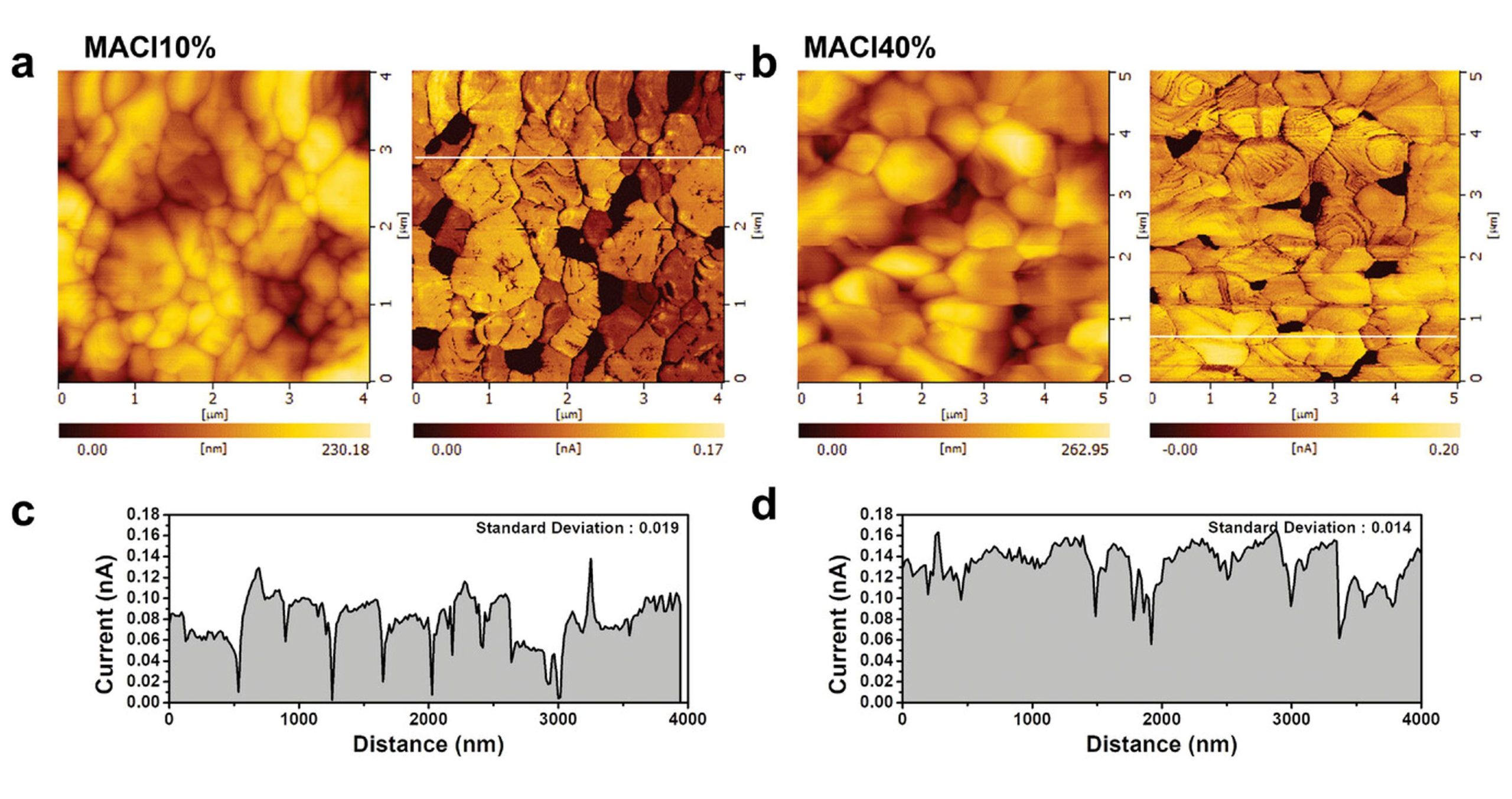
The electrical characterizations with atomic force microscopy (AFM) and conductive atomic force microscopy ( C-AFM) were done to measure the local conductance of FAPbI3 films. All measurements were performed under illumination (green LED) with a 1.3 V bias using a Pt-coated C-AFM probe (NanoWorld PlatinumIridium coated Pointprobe®CONTPt ). FTO was used for the conductive substrates. *
Conductive atomic force microscopy (C-AFM) indicated much more homogeneous photocurrent generation along the surface of (100) preferentially oriented layers. *
Figure 4 from Sooeun Shin et al. 2023 “Kinetic-Controlled Crystallization of α-FAPbI3 Inducing Preferred Crystallographic Orientation Enhances Photovoltaic Performance”: Electrical properties of (100)-oriented α-FAPbI3 thin films. a,b) Surface topography and photocurrent measurement by C-AFM of MACl10% and MACl40%. Measurements were taken under illumination (green LED) with a 1.3 V bias. Current images indicate that photocurrents were induced grain by grain, as each grain showed a distinct photocurrent. The photocurrent deviation for each grain is larger in MACl10% than in MACl40%, which shows a similar photocurrent grain by grain. c,d) Current line profile extracted from the current image (a and b). The standard deviation calculated from the magnitude of the photocurrent in each grain is displayed in the inset (0.019 and 0.014 nA for MACl10% and MACl40%, respectively). A low photocurrent was exhibited at the grain boundaries in both MACl10% and MACl40%. The dark areas measured within the current images are most likely distributed between grain edges. This may be caused by the formation of PbI2 or the loss of contact between the grain and the conducting substrate.
*Sooeun Shin, Seongrok Seo, Seonghwa Jeong, Anir S. Sharbirin, Jeongyong Kim, Hyungju Ahn, Nam-Gyu Park and Hyunjung Shin Kinetic-Controlled Crystallization of α-FAPbI3 Inducing Preferred Crystallographic Orientation Enhances Photovoltaic Performance
Advanced Science, Volume 10, Issue 14, May 17, 2023, 2300798
DOI: https://doi.org/10.1002/advs.202300798
Open Access The article “Kinetic-Controlled Crystallization of α-FAPbI3 Inducing Preferred Crystallographic Orientation Enhances Photovoltaic Performance” Sooeun Shin, Seongrok Seo, Seonghwa Jeong, Anir S. Sharbirin, Jeongyong Kim, Hyungju Ahn, Nam-Gyu Park and Hyunjung Shin is licensed under a Creative Commons Attribution 4.0 International License, which permits use, sharing, adaptation, distribution and reproduction in any medium or format, as long as you give appropriate credit to the original author(s) and the source, provide a link to the Creative Commons license, and indicate if changes were made. The images or other third party material in this article are included in the article’s Creative Commons license, unless indicated otherwise in a credit line to the material. If material is not included in the article’s Creative Commons license and your intended use is not permitted by statutory regulation or exceeds the permitted use, you will need to obtain permission directly from the copyright holder. To view a copy of this license, visit http://creativecommons.org/licenses/by/4.0/.