Ferroelectric domains and phase transition of sol-gel processed epitaxial Sm-doped BiFeO3 (001) thin films

Read how Nanoworld Arrow-EFM AFM probes were used in the paper “Ferroelectric domains and phase transition of sol-gel processed epitaxial Sm-doped BiFeO3 (001) thin films” in which the authors Zhen Zhou, Wie Sun, Zhenyu Liao, Shuai Ning, Jing Zhu and Jing-Feng Li:

  • prepared 12% Sm-doped BiFeO3 epitaxial thin films on Nb-doped SrTiO3 (001) substrate via a sol-gel method
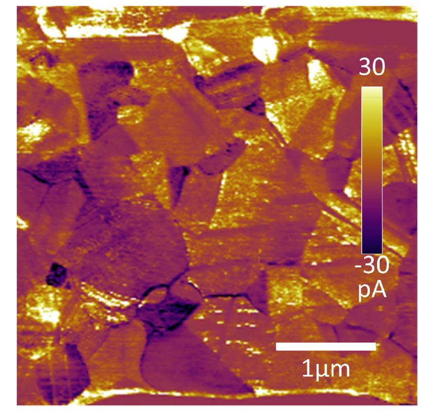
  • used PFM (piezoresponse force microscopy) to characterize the in-situ ferroelectric domain evolution from room temperature to 200 °C
  • illustrated a phase transition from ferroelectric to antiferroelectric phase by SS-PFM and found a significant piezoelectric response at the phase boundary

Their work revealed the origin of the high piezoresponse of Sm-doped BiFeO3 thin films at the morphotropic phase boundary (MPB).*

A PtIr-coated NanoWorld Arrow-EFM cantilever with a nominal spring constant of 2.8 N/m and a typical resonant frequency of 75 kHz was used in all imaging modes mentioned in the article.

Figure 3 from “Ferroelectric domains and phase transition of sol-gel processed epitaxial Sm-doped BiFeO3 (001) thin films” by Zhen Zhou et al. : PFM scanning results of the sample at 20 °C, 80 °C, 140 °C and 200 °C, (a)-(d) out-of-plane phase, (e)-(h) out-of-plane amplitude, (i)-(l) in-plane phase, and (m)-(p) in-plane amplitude. NanoWorld Arrow-EFM AFM probes were used in all imaging modes.
Figure 3 from “Ferroelectric domains and phase transition of sol-gel processed epitaxial Sm-doped BiFeO3 (001) thin films” by Zhen Zhou et al. : PFM scanning results of the sample at 20 °C, 80 °C, 140 °C and 200 °C, (a)-(d) out-of-plane phase, (e)-(h) out-of-plane amplitude, (i)-(l) in-plane phase, and (m)-(p) in-plane amplitude.


*Zhen Zhou, Wie Sun, Zhenyu Liao, Shuai Ning, Jing Zhu, Jing-Feng Li
Ferroelectric domains and phase transition of sol-gel processed epitaxial Sm-doped BiFeO3 (001) thin films

Journal of Materiomics, Volume 4, Issue 1, March 2018, Pages 27-34
DOI: https://doi.org/10.1016/j.jmat.2017.11.002

Please follow this external link if you would like to read the full article: https://www.sciencedirect.com/science/article/pii/S2352847817300631

Open Access The article “Ferroelectric domains and phase transition of sol-gel processed epitaxial Sm-doped BiFeO3 (001) thin films” by Zhen Zhou, Wie Sun, Zhenyu Liao, Shuai Ning, Jing Zhu and Jing-Feng Li is licensed under a Creative Commons Attribution 4.0 International License, which permits use, sharing, adaptation, distribution and reproduction in any medium or format, as long as you give appropriate credit to the original author(s) and the source, provide a link to the Creative Commons license, and indicate if changes were made. The images or other third party material in this article are included in the article’s Creative Commons license, unless indicated otherwise in a credit line to the material. If material is not included in the article’s Creative Commons license and your intended use is not permitted by statutory regulation or exceeds the permitted use, you will need to obtain permission directly from the copyright holder. To view a copy of this license, visit http://creativecommons.org/licenses/by/4.0/.


Direct AFM-based nanoscale mapping and tomography of open-circuit voltages for photovoltaics

In the article cited below Katherine Atamanuk, Justin Luria and Bryan D. Huey present “a new approach for directly mapping VOC (open-circuit voltage) with nanoscale resolution, requiring a single, standard-speed AFM scan. This leverages the concept of the proportional-integral-derivative (PID) feedback loop that underpins nearly all AFM topography imaging.”*

NanoWorld™ Pointprobe® CDT-NCHR conductive diamond coated silicon AFM probes were used in the described CT-AFM experiment.

Supporting information for «Direct AFM-based nanoscale mapping and tomography of open-circuit voltages for photovoltaics”: Figure S1: Representative quasi-VOC* image from the measured photocurrent upon illumination during an applied voltage fixed at 700 mV. NANOSENSORS conductive diamond coated CDT-NCHR AFM probes were used in the described CT-AFM experiment
Supporting information for «Direct AFM-based nanoscale mapping and tomography of open-circuit voltages for photovoltaics”: Figure S1: Representative quasi-VOC* image from the measured photocurrent upon illumination during an applied voltage fixed at 700 mV.

“Cadmium Telluride (CdTe) is an inexpensive thin-film photovoltaic with ca. 5% of the 2017 global market share for solar cells. To optimize the efficiency and reliability of these, or any electronic devices, a thorough understanding of their composition, microstructure, and performance is necessary as a function of device design, processing, and in-service conditions. Atomic force microscopy (AFM) has been a valuable tool for such characterization, especially of materials properties and device performance at the nanoscale. In the case of thin-film solar cells, local photovoltaic (PV) properties such as the open-circuit voltage, photocurrent, and work function have been demonstrated to vary by an order of magnitude, or more, within tens of nanometers […] Recently, property mapping with high spatial resolution by AFM has been further combined with the ability to serially mill a surface, in order to reveal underlying surface structures and uniquely develop three-dimensional (3D) nanoscale property maps. The most notable examples are based on pure current detection with the AFM to resolve conduction pathways in filamentary semiconducting devices and interconnects […], and tomographic AFM of photocurrents in polycrystalline solar cells during in situ illumination […].”*

*Katherine Atamanuk, Justin Luria, Bryan D. Huey
Direct AFM-based nanoscale mapping and tomography of open-circuit voltages for photovoltaics
Beilstein Journal of Nanotechnology 2018, 9, 1802–1808.
doi: 10.3762/bjnano.9.171

The article cited above is part of the Thematic Series “Scanning probe microscopy for energy-related materials”.

Please follow this external link for the full article: https://www.beilstein-journals.org/bjnano/articles/9/171

The article “Direct AFM-based nanoscale mapping and tomography of open-circuit voltages for photovoltaics” by Atamanuk et. al is an Open Access article under the terms of the Creative Commons Attribution License (http://creativecommons.org/licenses/by/4.0), which permits unrestricted use, distribution, and reproduction in any medium, provided the original work is properly cited.

Ferroelectric Domain Studies of Patterned (001) BiFeO3 by Angle-Resolved Piezoresponse Force Microscopy

Figure 1 from "Ferroelectric Domain Studies of Patterned (001) BiFeO 3 by Angle- Resolved Piezoresponse Force Microscopy": Patterned mesas are separated from the continuous film by lithography, as shown in the AFM topography image. (b) Schematic drawing of the atomic structure of BFO with angle-resolved polarization models. The Fe (red sphere) atom can be displaced towards twelve possible polarization orientations with respect to its centrosymmetric position. (c) AR-PFM domain map of a 1.2 × 1.2 μm2 area of unpatterned BFO film, corresponding to the black dashed area in (a). (d) The area distribution of each polarization variant according to angle relative to the [100] direction. (e) The average area of stable and meta-stable polarization variants.
Figure 1 from Seungbum Hong et al. “Ferroelectric Domain Studies of
Patterned (001) BiFeO3 by Angle-Resolved Piezoresponse Force Microscopy”:
Patterned mesas are separated from the continuous film by lithography, as shown in the AFM topography image.
(b) Schematic drawing of the atomic structure of BFO with angle-resolved polarization models. The Fe (red sphere) atom can be displaced towards twelve possible polarization orientations with respect to its centrosymmetric position. (c) AR-PFM domain map of a 1.2 × 1.2 μm2 area of unpatterned BFO film, corresponding to the black dashed area in (a). (d) The area distribution of each polarization variant according to angle relative to the [100] direction. (e) The average area of stable and meta-stable polarization variants.
NanoWorld EFM PtIr coated probes were used for the PFM measurements mentioned in this brand new publication on ferroelectric domain imaging of patterned BFO thin films in Scientific Reports.
Congratulations to the authors!
 #afmprobes #atomicforcemicroscopy #afmtips #AFM

Bumsoo Kim, Frank P. Barrows, Yogesh Sharma, Ram S. Katiyar, Charudatta Phatak, Amanda K. Petford-Long, Seokwoo Jeon, Seungbum Hong
Scientific Reports (2018) 8:20, DOI:10.1038/s41598-017-18482-9
For the full article please follow this external link:


Open Access
This article is licensed under a Creative Commons Attribution 4.0 International
License, which permits use, sharing, adaptation, distribution and reproduction in any medium or format, as long as you give appropriate credit to the original author(s) and the source, provide a link to the Creative Commons license, and indicate if changes were made. The images or other third party material in this
article are included in the article’s Creative Commons license, unless indicated otherwise in a credit line to the material. If material is not included in the article’s Creative Commons license and your intended use is not per-
mitted by statutory regulation or exceeds the permitted use, you will need to obtain permission directly from the copyright holder. To view a copy of this license, visit http://creativecommons.org/licenses/by/4.0/