Eom S, Kavle P, Kang D, Kim Y, Martin LW, Hong S
Unveiling the Nanoscale Dielectric Gap and Its Influence on Ferroelectric Polarization Switching in Scanning Probe Microscopy
Advanced Functional Materials. 2025 Mar;35(11):2406944
DOI: https://doi.org/10.1002/adfm.202406944
Jung H, Kim SH
Evolution of Electrical Degradation in Ternary Cathode Materials of Lithium-Ion Batteries
Available at SSRN 5163096
DOI: http://doi.org/10.2139/ssrn.5163096
Takasaka R, Umehara N, Tokoroyama T, Zhang R, Okamura K, Fukuda J, Hayashi T, Abe K, Wakamatsu S
Abnormal Wear due to Synergistic Effects of Corrosion and Cavitation in High-Speed Flow of Glycol-Based Hydraulic Fluid Valve Surfaces
Tribology Online. 2025 Jun 30;20(2):100-9
DOI: https://doi.org/10.2474/trol.20.100
Cho M, yeon Park S, Jung H, Kim SH
Characterization of identical lithium-ion battery electrodes before and after charge/discharge cycles via in-plane large-area polishing
Nanotechnology. 2024 Oct 4;35(50):505401
DOI: https://doi.org/10.1088/1361-6528/ad7f60
Tokoroyama T, Horikawa S, Mimata J, Umehara N, Murashima M
Effect of Water on Wear of DLC Coatings in High Temperature and Pressurized Ethanol
Tribology Letters. 2024 Dec;72(4):111
DOI: https://doi.org/10.1007/s11249-024-01910-z
Shen G, Zhu L, Wang Z, Zhao J, Shu L
Tuning Self-Polarization of Epitaxial BiFeO3 Thin Films through Interface Effects
ACS Applied Materials & Interfaces. 2024 Dec 9;16(50):70038-46
DOI: https://doi.org/10.1021/acsami.4c14995
Cho M, Lee SH, Yuk E, Park H, Kim SH
Nanoscale electrical characterization of ambient-induced surface impurities on high-nickel cathode materials for lithium-ion batteries
Journal of Alloys and Compounds. 2023 Nov 10;963:171215
DOI: https://doi.org/10.1016/j.jallcom.2023.171215
Itasaka H, Liu Z, Mimura KI, Hamamoto K
Ultra-thin barium titanate nanocrystal monolayer capacitor with graphene electrode
Applied Physics Letters. 2023 Aug 28;123(9)
DOI: https://doi.org/10.1063/5.0156549
Nath R, Polomoff NA, Song J, Moran TJ, Ramesh R, Huey BD
Nanoscale Activation Energy Mapping and Leveraging for Accelerating Ferroelectric Domain Nucleation and Growth
Advanced Electronic Materials. 2022 Jun;8(6):2101389
DOI: https://doi.org/10.1002/aelm.202101389
Aryeetey F, Pourianejad S, Ayanbajo O, Nowlin K, Ignatova T, Aravamudhan S
Bandgap recovery of monolayer MoS 2 using defect engineering and chemical doping
RSC advances. 2021;11(34):20893-8
DOI: https://doi.org/10.1039/D1RA02888J
Yang Y, Xi Z, Dong Y, Zheng C, Hu H, Li X, Jiang Z, Lu WC, Wu D, Wen Z
Spin-filtering ferroelectric tunnel junctions as multiferroic synapses for neuromorphic computing
ACS Applied Materials & Interfaces. 2020 Dec 7;12(50):56300-9
DOI: https://doi.org/10.1021/acsami.0c16385
Li R, Xu Y, Song J, Wang P, Li C, Wu D
Preparation and characterization of a flexible ferroelectric tunnel junction
Applied Physics Letters. 2020 Jun 1;116(22)
DOI: https://doi.org/10.1063/5.0006638
Tian G, Yang W, Song X, Zheng D, Zhang L, Chen C, Li P, Fan H, Yao J, Chen D, Fan Z
Manipulation of conductive domain walls in confined ferroelectric nanoislands
Advanced Functional Materials. 2019 Aug;29(32):1807276
DOI: https://doi.org/10.1002/adfm.201807276
Park SY, Baek WJ, Lee SY, Seo JA, Kang YS, Koh M, Kim SH
Probing electrical degradation of cathode materials for lithium-ion batteries with nanoscale resolution
Nano Energy. 2018 Jul 1;49:1-6
DOI: https://doi.org/10.1016/j.nanoen.2018.04.005
Kim SH, Kim YS, Baek WJ, Heo S, Han S, Jung H
Nanoscale electrical resistance imaging of solid electrolyte interphases in lithium-ion battery anodes
Journal of Power Sources. 2018 Dec 15;407:1-5.
DOI: https://doi.org/10.1016/j.jpowsour.2018.10.027
Li C, Shen Y, Huang R, Kumamoto A, Chen S, Dai C, Yoshiya M, Fujii S, Funai K, Fisher CA, Wang Y.
Hierarchically structured thermoelectric materials in quaternary system Cu–Zn–Sn–S featuring a mosaic-type nanostructure
ACS Applied Nano Materials. 2018 May 25;1(6):2579-88
DOI: https://doi.org/10.1021/acsanm.8b00278
Fan Z, Fan H, Yang L, Li P, Lu Z, Tian G, Huang Z, Li Z, Yao J, Luo Q, Chen C
Resistive switching induced by charge trapping/detrapping: a unified mechanism for colossal electroresistance in certain Nb: SrTiO 3-based heterojunctions
Journal of Materials Chemistry C. 2017;5(29):7317-27
DOI: https://doi.org/10.1039/C7TC02197F
Kutes Y, Luria J, Sun Y, Moore A, Aguirre BA, Cruz-Campa JL, Aindow M, Zubia D, Huey BD
Ion-damage-free planarization or shallow angle sectioning of solar cells for mapping grain orientation and nanoscale photovoltaic properties
Nanotechnology. 2017 Apr 11;28(18):185705
DOI: https://doi.org/10.1088/1361-6528/aa67c2
Xi Z, Ruan J, Li C, Zheng C, Wen Z, Dai J, Li A, Wu D
Giant tunnelling electroresistance in metal/ferroelectric/semiconductor tunnel junctions by engineering the Schottky barrier
Nature communications. 2017 May 17;8(1):15217
DOI: https://doi.org/10.1038/ncomms15217
Luria J, Kutes Y, Moore A, Zhang L, Stach EA, Huey BD
Charge transport in CdTe solar cells revealed by conductive tomographic atomic force microscopy
Nature energy. 2016 Sep 26;1(11):1-6
DOI: https://doi.org/10.1038/nenergy.2016.150
Wen Z, Qiu X, Li C, Zheng C, Ge X, Li A, Wu D
Mechanical switching of ferroelectric polarization in ultrathin BaTiO3 films: The effects of epitaxial strain
Applied Physics Letters. 2014 Jan 27;104(4).
DOI: https://doi.org/10.1063/1.4863855
Zhang Q, Valanoor N, Standard O
Chemical solution deposition derived (001)-oriented epitaxial BiFeO3 thin films with robust ferroelectric properties using stoichiometric precursors
Journal of Applied Physics. 2014 Aug 14;116(6)
DOI: https://doi.org/10.1063/1.4891311
Pantel D, Lu H, Goetze S, Werner P, Jik Kim D, Gruverman A, Hesse D, Alexe M
Tunnel electroresistance in junctions with ultrathin ferroelectric Pb (Zr0. 2Ti0. 8) O3 barriers
Applied Physics Letters. 2012 Jun 4;100(23).
DOI: https://doi.org/10.1063/1.4726120
Kumar A, Shivareddy SG, Correa M, Resto O, Choi Y, Cole MT, Katiyar RS, Scott JF, Amaratunga GA, Lu H, Gruverman A
Ferroelectric–carbon nanotube memory devices
Nanotechnology. 2012 Mar 30;23(16):165702
DOI: https://doi.org/10.1088/0957-4484/23/16/165702
Totokawa M, Tani T, Yoshimura M, Yamashita S, Morikawa K, Mitsuoka Y, Nonaka T
Chemical and Piezoresistive Microanalyses at the Interface of RuO2–Glass Diffusion Pairs
Journal of the American Ceramic Society. 2010 Feb;93(2):481-7
DOI: https://doi.org/10.1111/j.1551-2916.2009.03403.x
Rommel M, Spoldi G, Yanev V, Beuer S, Amon B, Jambreck J, Petersen S, Bauer AJ, Frey L
Comprehensive study of focused ion beam induced lateral damage in silicon by scanning probe microscopy techniques
Journal of Vacuum Science & Technology B. 2010 May 1;28(3):595-607
DOI: https://doi.org/10.1116/1.3431085


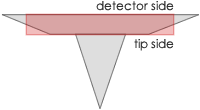 A trapezoidal cross section of the AFM cantilever and therefore 30% wider (e.g. NCH) AFM cantilever detector side result in easier and faster laser adjustment. Additionally, because there is simply more space to place and reflect the laser beam, a higher SUM signal is reached.

 POINTPROBE®
 ARROW™
 ULTRA-SHORT CANTILEVERS
 PYREX-NITRIDE
 COATINGS