Alzheimer’s disease (AD) is the most frequent neurodegenerative disorder in the elderly aged over 65.*
The extracellular accumulation of beta-amyloid (Aβ) aggregates in the brain is considered as the major event worsening the AD symptoms, but its underlying reason has remained unclear.
In the article „Lateral Piezoelectricity of Alzheimer‘s Aβ Aggregates“ by Jinhyeong Jang, Soyun Joo, Jiwon Yeom, Yonghan Jo, Jingshu Zhang, Seungbum Hong and Chan Beum Park the piezoelectric characteristics of Aβ aggregates are revealed.
The vector piezoresponse force microscopy (PFM) analysis results exhibit that Aβ fibrils have spiraling piezoelectric domains along the length and a lateral piezoelectric constant of 44.1 pC N-1. Also, the continuous sideband Kelvin probe force microscopy (KPFM) images display that the increment of charge-induced surface potential on a single Aβ fibril is allowed to reach above +1700 mV in response to applied forces.
These findings shed light on the peculiar mechano-electrical surface properties of pathological Aβ fibrils that exceed those of normal body components.*
Both KPFM and nanoindentation measurements were performed using a chemically inert conductive diamond AFM tip. (NanoWorld Pointprobe CDT-FMR).
Vertical and lateral PFM images of Aβ fibrils were obtained by scanning probe microscopy with a platinum/iridium-coated silicon cantilever ( NanoWorld Pointprobe® CONTPt ). The scanning angle of the PFM cantilever was set to zero, with scan rate of 0.5 Hz and loading force of 10 nN. This setup minimized electrostatic contributions to the torsional movement of the tip, allowing measurements to focus on the shear electromechanical effects of Aβ fibrils. Vertical and lateral drive frequencies were 53 kHz and 309 kHz, respectively.*
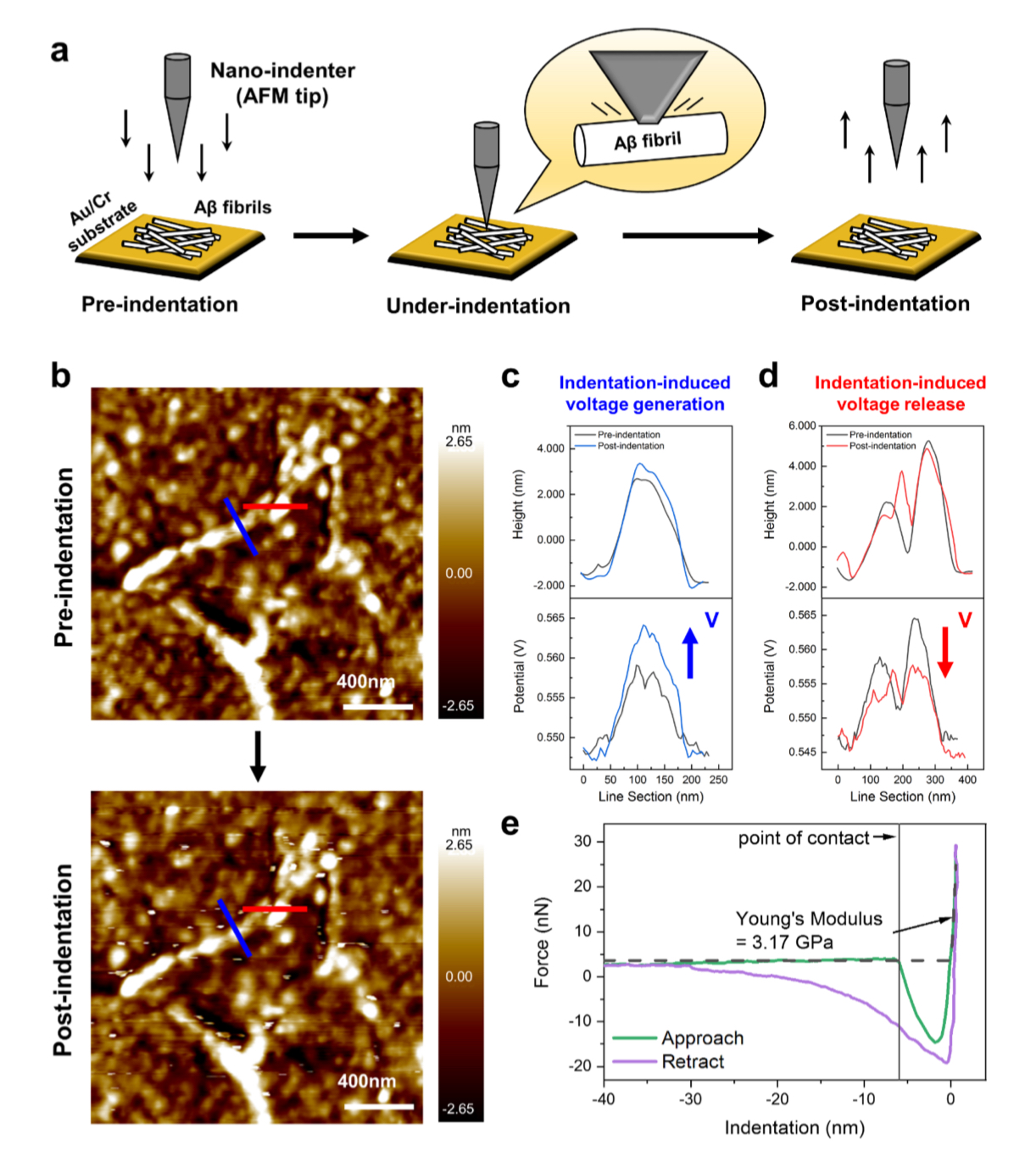
Nanoindentation test result of Aβ fibrils. Direct piezoelectric effects are tested by measuring the surface potential change before and after nano-indentation of Aβ fibrils.
(A) Schematic illustration of the nanoindentation test for Aβ fibrils coated on an Au/Cr substrate.
(B) Topgraphy of Aβ fibrils acquired before and after applying nanoindentation. The post-indentation image shows white spots resulting from physical interactions between the AFM tip and the sample, while the approximate structure of the Aβ fibrils remains intact. Height and potential line sections obtained fom the (c) blue and (d) red lines are shown in the topgraphy of Aβ fibrils. The height remains unchanged, while electrical voltage increment and decrement were observed at the blue and red lines, respectively.
(D) During the nanoindentation the Young‘s modulus of Aβ – fibrils was measured to be 3.17 GPa, closely approxmating the literature (Nanoscale 4, 4426-4429 (2012). Both KPFM and nanoindentation measurements were performed using a chemically inert conductive diamond AFM tip (CDT-FMR, NanoWorld, Switzerland). Collected force curves were analyzed using the Hertz model to estimate the elastic moduli.
*Jinhyeong Jang, Soyun Joo, Jiwon Yeom, Yonghan Jo, Jingshu Zhang, Seungbum Hong and Chan Beum Park
Lateral Piezoelectricity of Alzheimer‘s Aβ Aggregates
Advanced Science, Volume 11, Issue 39, October 024, 2406678
DOI: https://doi.org/10.1002/advs.202406678
Open Access The article “Lateral Piezoelectricity of Alzheimer‘s Aβ Aggregates” byJinhyeong Jang, Soyun Joo, Jiwon Yeom, Yonghan Jo, Jingshu Zhang, Seungbum Hong and Chan Beum Park is licensed under a Creative Commons Attribution 4.0 International License, which permits use, sharing, adaptation, distribution and reproduction in any medium or format, as long as you give appropriate credit to the original author(s) and the source, provide a link to the Creative Commons license, and indicate if changes were made. The images or other third party material in this article are included in the article’s Creative Commons license, unless indicated otherwise in a credit line to the material. If material is not included in the article’s Creative Commons license and your intended use is not permitted by statutory regulation or exceeds the permitted use, you will need to obtain permission directly from the copyright holder. To view a copy of this license, visit http://creativecommons.org/licenses/by/4.0/.