Topological objects and defects (e.g. skyrmions, domain walls, vortices,) in condensed matters have attracted a lot of interest as a field for exploring emerging exotic phenomena and functionalities.*
In materials with ferroic order, these topological objects can also be manipulated and controlled by external fields without disrupting their host lattice, making them promising elemental building blocks for potential configurable topological nanoelectronics. *
Ferroelectric topological objects provide a promising area for investigating emerging physical properties that could potentially be utilized in future nanoelectronic devices. *
In the article “Quasi-one-dimensional metallic conduction channels in exotic ferroelectric topological defects” Wenda Yang, Guo Tian, Yang Zhang, Fei Xue, Dongfeng Zheng, Luyong Zhang, Yadong Wang, Chao Chen, Zhen Fan, Zhipeng Hou, Deyang Chen, Jinwei Gao, Min Zeng, Minghui Qin, Long-Qing Chen, Xingsen Gao and Jun-Ming Liu demonstrate the existence of metallic conduction superfine (<3 nm) channels in two types of exotic topological defects, namely a quadrant vortex core or simply vortex core and a quadrant center domain core or simply center core, in an array of BiFeO3 (BFO) nanoislands.*
The authors discover via the phase-field simulation that the superfine metallic conduction channels along the center cores arise from the screening charge carriers confined at the core region, whereas the high conductance of vortex cores results from a field-induced twisted state. These conducting channels can be reversibly created and deleted by manipulating the two topological states via electric field, leading to an apparent electroresistance effect with an on/off ratio higher than 103.*
The findings by Wenda Yang et al. open up the possibility of using these functional one-dimensional topological objects in high-density nanoelectronic devices, e.g. nonvolatile memory.*
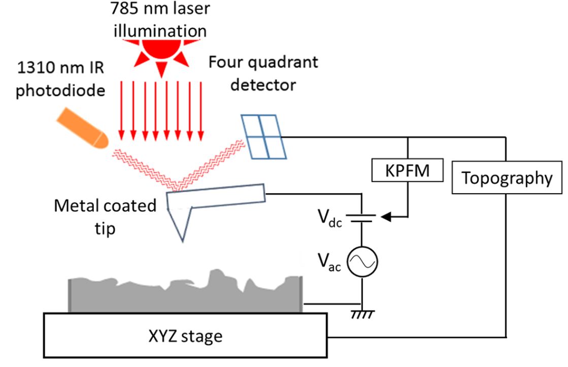
NanoWorld PlatinumIdridium5 coated Arrow-EFM AFM probes were used to examine the domain structures by vector piezoresponse force microscopy (PFM). By using vector PFM mode, the authors could simultaneously map the vertical and lateral piezoresponse signals from the nanoisland one by one.*
NanoWorld Conductive Diamond coated AFM probes CDT-NCHR were used for the conductive current distribution maps, current–voltage (I–V) measurements that were characterized by conductive atomic force microscopy (C-AFM).
The domain structures and corresponding conductive properties for both a vortex and a center topological states confined in two nanoislands.
a, b PFM and C-AFM images for both a vortex state (a) and a center state (b), the micrographs from the left to the right are PFM vertical phase images illustrating the uniform upward vertical polarization components for both nanoislands, the PFM lateral phase images recorded at sample rotation of 0o and 90o to evaluate the directions of lateral polarization components respectively along x axis ([100] axis) and y axis ([100] axis), the lateral polarization vector direction maps derived from the PFM data, and corresponding C-AFM maps. The thick arrows aside the PFM images mark the directions of the cantilever for each PFM scan, and the fine arrows inside the images mark the directions of polarization components perpendicular to the directions of the cantilever. c, d Extracted current spatial profiles from the C-AFM maps for both the vortex (c) and the center (d) cores, extracted from a and b, respectively. The inserts in c and d illustrate the C-AFM maps and schematic local polarization configurations for the two topological cores. e Temperature-dependent conductive current (I–V) curves for both topological cores and domain walls.*
*Wenda Yang, Guo Tian, Yang Zhang, Fei Xue, Dongfeng Zheng, Luyong Zhang, Yadong Wang, Chao Chen, Zhen Fan, Zhipeng Hou, Deyang Chen, Jinwei Gao, Min Zeng, Minghui Qin, Long-Qing Chen, Xingsen Gao and Jun-Ming Liu
Quasi-one-dimensional metallic conduction channels in exotic ferroelectric topological defects
Nature Communications volume 12, Article number: 1306 (2021)
DOI: https://doi.org/10.1038/s41467-021-21521-9
Please follow this external link to read the full article: https://rdcu.be/cg0JY
Open Access : The article “Quasi-one-dimensional metallic conduction channels in exotic ferroelectric topological defects” by Wenda Yang, Guo Tian, Yang Zhang, Fei Xue, Dongfeng Zheng, Luyong Zhang, Yadong Wang, Chao Chen, Zhen Fan, Zhipeng Hou, Deyang Chen, Jinwei Gao, Min Zeng, Minghui Qin, Long-Qing Chen, Xingsen Gao and Jun-Ming Liu is licensed under a Creative Commons Attribution 4.0 International License, which permits use, sharing, adaptation, distribution and reproduction in any medium or format, as long as you give appropriate credit to the original author(s) and the source, provide a link to the Creative Commons license, and indicate if changes were made. The images or other third party material in this article are included in the article’s Creative Commons license, unless indicated otherwise in a credit line to the material. If material is not included in the article’s Creative Commons license and your intended use is not permitted by statutory regulation or exceeds the permitted use, you will need to obtain permission directly from the copyright holder. To view a copy of this license, visit https://creativecommons.org/licenses/by/4.0/.