Tunable and parabolic piezoelectricity in hafnia under epitaxal strain

Piezoelectrics are a class of functional materials that have been extensively used for application in modern electro-mechanical and mechatronics technologies. *

The sign of longitudinal piezoelectric coefficients is typically positive but recently a few ferroelectrics, such as ferroelectric polymer poly(vinylidene fluoride) and van der Waals ferroelectric CuInP2S6, were experimentally found to have negative piezoelectricity.

In the article “Tunable and parabolic piezoelectricity in hafnia under epitaxial strain” Hao Cheng, Peijie Jiao, Jian Wang, Mingkai Qing, Yu Deng, Jun-Ming Liu, Laurent Bellaiche, Di Wu and Yurong Yang, using first-principles calculation and measurements, show that the sign of the longitudinal linear piezoelectric coefficient of HfO2 can be tuned from positive to negative via epitaxial strain. *

Nonlinear and even parabolic piezoelectric behaviors are further found at tensile epitaxial strain. *

This parabolic piezoelectric behavior implies that the polarization decreases when increasing the magnitude of either compressive or tensile longitudinal strain, or, equivalently, that the strain increases when increasing the magnitude of electric field being either parallel or antiparallel to the direction of polarization. The unusual piezoelectric effects are from the chemical coordination of the active oxygen atoms. *

These striking piezoelectric features of positive and negative sign, as well as linear and parabolical behaviors, expand the current knowledge in piezoelectricity and broaden the potential of piezoelectric applications towards electro-mechanical and communications technology. *

NanoWorld Pt/Ir coated Pointprobe® EFM AFM probes were used for the sample characterization by switching spectroscopy PFM measurements.

Switching spectroscopy PFM measurements were performed on the bare HZO film surface at room temperature with Nanoworld Pointprobe® EFM in a commercially available atomic force microscope, while the LSMO electrode was grounded.
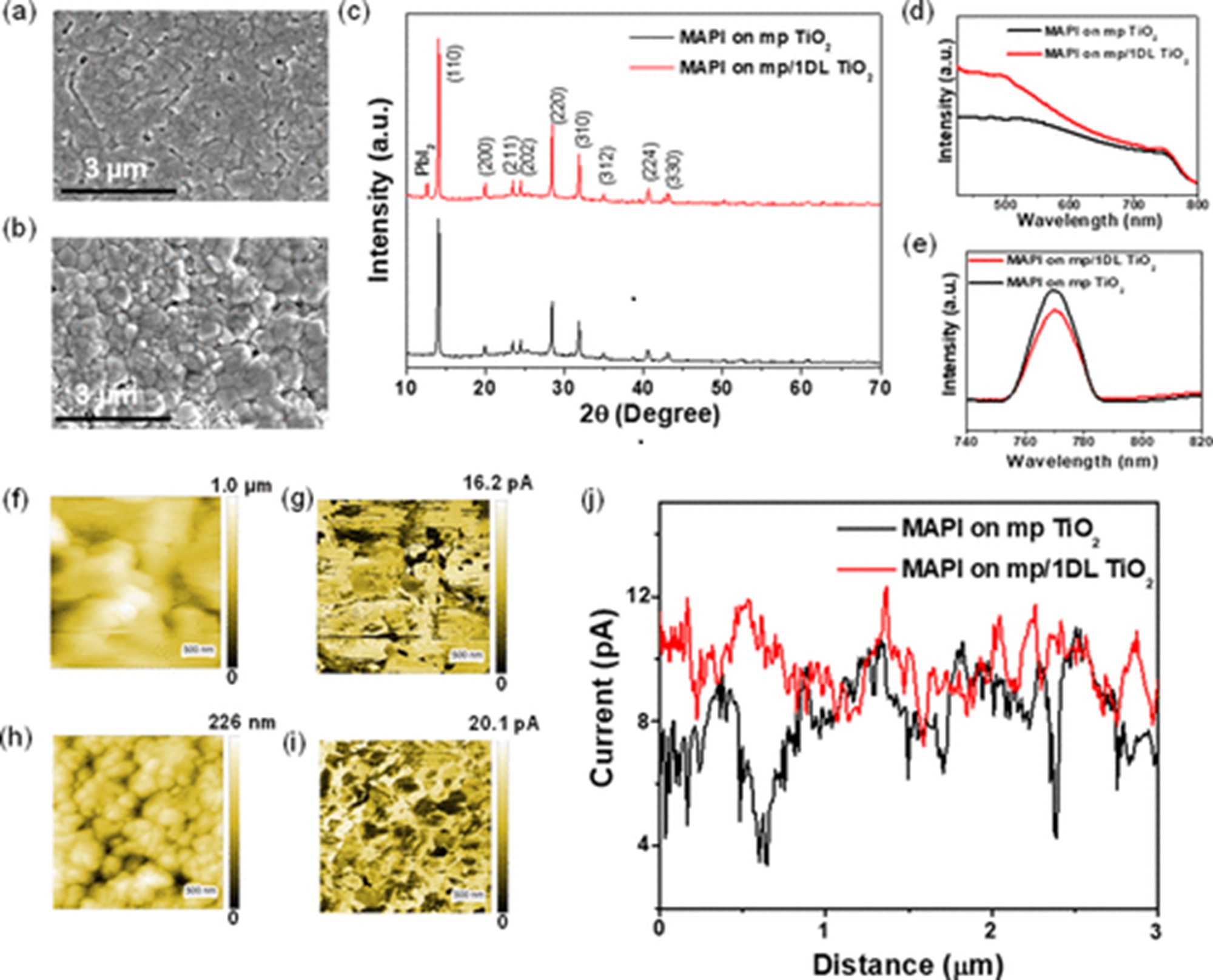
Fig. 5 from Hao Cheng et al. (2024) “Tunable and parabolic piezoelectricity in hafnia under epitaxial strain”: [111]-oriented HZO films grown on (110) LAO substrates with different thicknesses of LSMO buffer layers.a XRD θ-2θ patterns of HZO films deposited on (110)-oriented LAO with 20-, 33-, 66-nm-thick LSMO buffer layers. b PFM phase loops of the HZO films deposited on 20-, 33- and 66-nm-thick LSMO buffered LAO substrates. c–e Reciprocal space mappings around the (310) spot of HZO/LSMO/LAO with c 20-, d 33-, and e 66-nm-thick LSMO buffer layers. NanoWorld Pt/Ir coated Pointprobe® EFM AFM probes the sample characterization by switching spectroscopy PFM measurements.

Fig. 5 from Hao Cheng et al. (2024) “Tunable and parabolic piezoelectricity in hafnia under epitaxial strain”: [111]-oriented HZO films grown on (110) LAO substrates with different thicknesses of LSMO buffer layers.
a XRD θ-2θ patterns of HZO films deposited on (110)-oriented LAO with 20-, 33-, 66-nm-thick LSMO buffer layers. b PFM phase loops of the HZO films deposited on 20-, 33- and 66-nm-thick LSMO buffered LAO substrates. c–e Reciprocal space mappings around the (310) spot of HZO/LSMO/LAO with c 20-, d 33-, and e 66-nm-thick LSMO buffer layers.
*Hao Cheng, Peijie Jiao, Jian Wang, Mingkai Qing, Yu Deng, Jun-Ming Liu, Laurent Bellaiche, Di Wu and Yurong Yang
Tunable and parabolic piezoelectricity in hafnia under epitaxial strain
Nature Communications volume 15, Article number: 394 (2024)
DOI: https://doi.org/10.1038/s41467-023-44207-w

Open Access  The article “ Tunable and parabolic piezoelectricity in hafnia under epitaxial strain ” by Hao Cheng, Peijie Jiao, Jian Wang, Mingkai Qing, Yu Deng, Jun-Ming Liu, Laurent Bellaiche, Di Wu and Yurong Yang is licensed under a Creative Commons Attribution 4.0 International License, which permits use, sharing, adaptation, distribution and reproduction in any medium or format, as long as you give appropriate credit to the original author(s) and the source, provide a link to the Creative Commons license, and indicate if changes were made. The images or other third party material in this article are included in the article’s Creative Commons license, unless indicated otherwise in a credit line to the material. If material is not included in the article’s Creative Commons license and your intended use is not permitted by statutory regulation or exceeds the permitted use, you will need to obtain permission directly from the copyright holder. To view a copy of this license, visit http://creativecommons.org/licenses/by/4.0/.

Interfacial Engineering with One-Dimensional Lepidocrocite TiO2-Based Nanofilaments for High-Performance Perovskite Solar Cells

The optimization of nonradiative recombination losses through interface engineering is key to the development of efficient, stable, and hysteresis-free perovskite solar cells (PSCs). *

In the article “Interfacial Engineering with One-Dimensional Lepidocrocite TiO2-Based Nanofilaments for High-Performance Perovskite Solar Cells”  Shrabani Panigrahi, Hussein O. Badr, Jonas Deuermeier, Santanu Jana, Elvira Fortunato, Rodrigo Martins and Michel W. Barsoum, for the first time in solar cell technology, present a novel approach to interface modification by employing one-dimensional lepidocrocite (henceforth referred to as 1DL) TiO2-based nanofilaments, NFs, between the mesoporous TiO2 (mp TiO2) and halide perovskite film in PSCs to improve both the efficiency and stability of the devices. *

The 1DLs can be easily produced on the kilogram scale starting with cheap and earth-abundant precursor powders, such as TiC, TiN, TiB2, etc., and a common organic base like tetramethylammonium hydroxide. Notably, the 1DL deposition influenced perovskite grain development, resulting in a larger grain size and a more compact perovskite layer. Additionally, it minimized trap centers in the material and reduced charge recombination processes, as confirmed by the photoluminescence analysis. *

The overall promotion led to an improved power conversion efficiency (PCE) from 13 ± 3.2 to 16 ± 1.8% after interface modification. The champion PCE for the 1DL-containing devices is 17.82%, which is higher than that of 16.17% for the control devices. *

The passivation effect is further demonstrated by evaluating the stability of PSCs under ambient conditions, wherein the 1DL-containing PSCs maintain ∼87% of their initial efficiency after 120 days. *

The article not only presents cost-effective, novel, and promising materials for cathode interface engineering but also an effective approach to achieve high-efficiency PSCs with long-term stability devoid of encapsulation. *

To get a deeper understanding of the enhanced photocurrent production within the perovskite layer, the authors used photoconductive atomic force microscopy (pcAFM) to map the photocurrent distribution at the nanoscale for the same perovskite layers on both types of ETLs. *

pcAFM measurements were taken in air with a commercially available Atomic Force Microscopy by using conductive PtIr-coated NanoWorld Pointprobe® CONTPt silicon AFM probes (typical resonance frequency = 13 kHz, typical spring constant = 0.2 N/m) and a current detector holder. A light source was used to light the samples. *

Figure 4 from Shrabani Panigrahi et al. 2024 “Interfacial Engineering with One-Dimensional Lepidocrocite TiO2-Based Nanofilaments for High-Performance Perovskite Solar Cells”:Characterization of the perovskite films (MAPbI3 is denoted as MAPI inside figure) deposited on mp TiO2 and mp/1DL ETLs: (a, b) FESEM micrographs, (c) XRD patterns, (d) UV/vis absorption, and (e) PL spectra. (f, h) AFM topography images and (g, i) corresponding pcAFM photocurrent images of the perovskite layers deposited on mp TiO2 and mp/1DL TiO2 ETLS, respectively. (j) Photocurrent line profiles across the perovskite layers. pcAFM measurements were taken in air using conductive PtIr-coated NanoWorld Pointprobe® CONTPt silicon AFM probes
Figure 4 from Shrabani Panigrahi et al. 2024 “Interfacial Engineering with One-Dimensional Lepidocrocite TiO2-Based Nanofilaments for High-Performance Perovskite Solar Cells”:
Characterization of the perovskite films (MAPbI3 is denoted as MAPI inside figure) deposited on mp TiO2 and mp/1DL ETLs: (a, b) FESEM micrographs, (c) XRD patterns, (d) UV/vis absorption, and (e) PL spectra. (f, h) AFM topography images and (g, i) corresponding pcAFM photocurrent images of the perovskite layers deposited on mp TiO2 and mp/1DL TiO2 ETLS, respectively. (j) Photocurrent line profiles across the perovskite layers.

*Shrabani Panigrahi, Hussein O. Badr, Jonas Deuermeier, Santanu Jana, Elvira Fortunato, Rodrigo Martins and Michel W. Barsoum
Interfacial Engineering with One-Dimensional Lepidocrocite TiO2-Based Nanofilaments for High-Performance Perovskite Solar Cells
ACS Omega 2024, 9, 51, 50820–50829
DOI: https://doi.org/10.1021/acsomega.4c09516

Open Access The article “Interfacial Engineering with One-Dimensional Lepidocrocite TiO2-Based Nanofilaments for High-Performance Perovskite Solar Cells” by Shrabani Panigrahi, Hussein O. Badr, Jonas Deuermeier, Santanu Jana, Elvira Fortunato, Rodrigo Martins and Michel W. Barsoum is licensed under a Creative Commons Attribution 4.0 International License, which permits use, sharing, adaptation, distribution and reproduction in any medium or format, as long as you give appropriate credit to the original author(s) and the source, provide a link to the Creative Commons license, and indicate if changes were made. The images or other third-party material in this article are included in the article’s Creative Commons license, unless indicated otherwise in a credit line to the material. If material is not included in the article’s Creative Commons license and your intended use is not permitted by statutory regulation or exceeds the permitted use, you will need to obtain permission directly from the copyright holder. To view a copy of this license, visit http://creativecommons.org/licenses/by/4.0/.

NanoWorld at MRS Fall Meeting & Exhibit 2024 this week

NanoWorld CEO Manfred Detterbeck is in Boston for the MRS Fall 2024 Meeting & Exhibit this week.
You’ll meet him at some of the sessions or at NanoAndMore USA booth no. 402.

If you’re there too feel free to say hi and have a chat about #AFMprobes with him.

NanoWorld AFM probes CEO Manfred Detterbeck in front of the MRS Logo at the MRS Fall 2024 at Hynes Convention Center in Boston.
Happy to be at MRS Fall 2024. Hope to see many of you here.