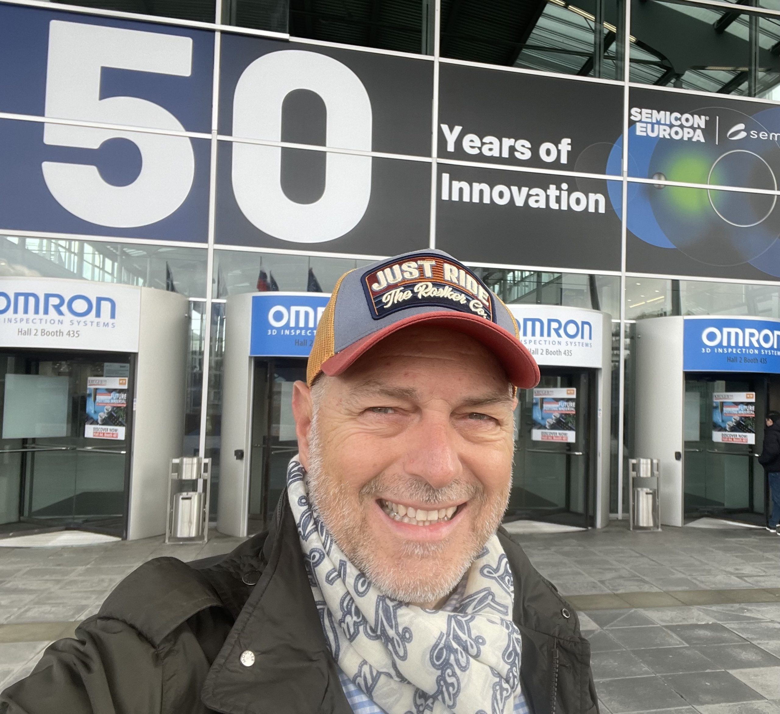
NanoWorld AG CEO Manfred Detterbeck is attending the 50th anniversary edition of #SEMICONEuropa (co-located with productronica), which will take place from November 18-21, 2025 in Munich, Germany.
Will you be there to celebrate too?
NanoWorld AG CEO Manfred Detterbeck is attending the 50th anniversary edition of #SEMICONEuropa (co-located with productronica), which will take place from November 18-21, 2025 in Munich, Germany.
Will you be there to celebrate too?
A reliable replacement of the Olympus®* AC160 –
Optimized Positioning with Maximum AFM Tip Visibility
NanoWorld AG is pleased to introduce the new Arrow-ACR AFM probe, developed to provide research professionals worldwide with a dependable alternative to the discontinued Olympus®* AC160 microcantilever.
The Arrow™ ACR (typical resonance frequency 300 kHz, typical force constant 26 N/m), combines identical mechanical properties as the
Olympus®* AC160 with the well-known Arrow AFM tip and cantilever geometry. Always positioned exactly at the end of the AFM cantilever, this AFM probe offers easy positioning of the AFM tip over the area of interest.
With their moderate stiffness (typical force constant 26 N/m) the Arrow™ ACR probes are particularly suitable for studying relatively soft materials, including various polymers. These AFM probes are designed to perform optimally in non-contact/Tapping™ mode in air, enabling detailed characterization of thin films, coatings, surface roughness, and localized defects.
Users can expect stable operation, high sensitivity and high-speed scanning capabilities, ensuring reproducible data across a wide range of applications.
For researchers seeking a seamless transition from the discontinued
Olympus®* AC160, the NanoWorld® Arrow™ ACR offers a reliable solution backed by NanoWorld’s manufacturing precision and quality control.
*Olympus® is a trademark of Olympus Corporation
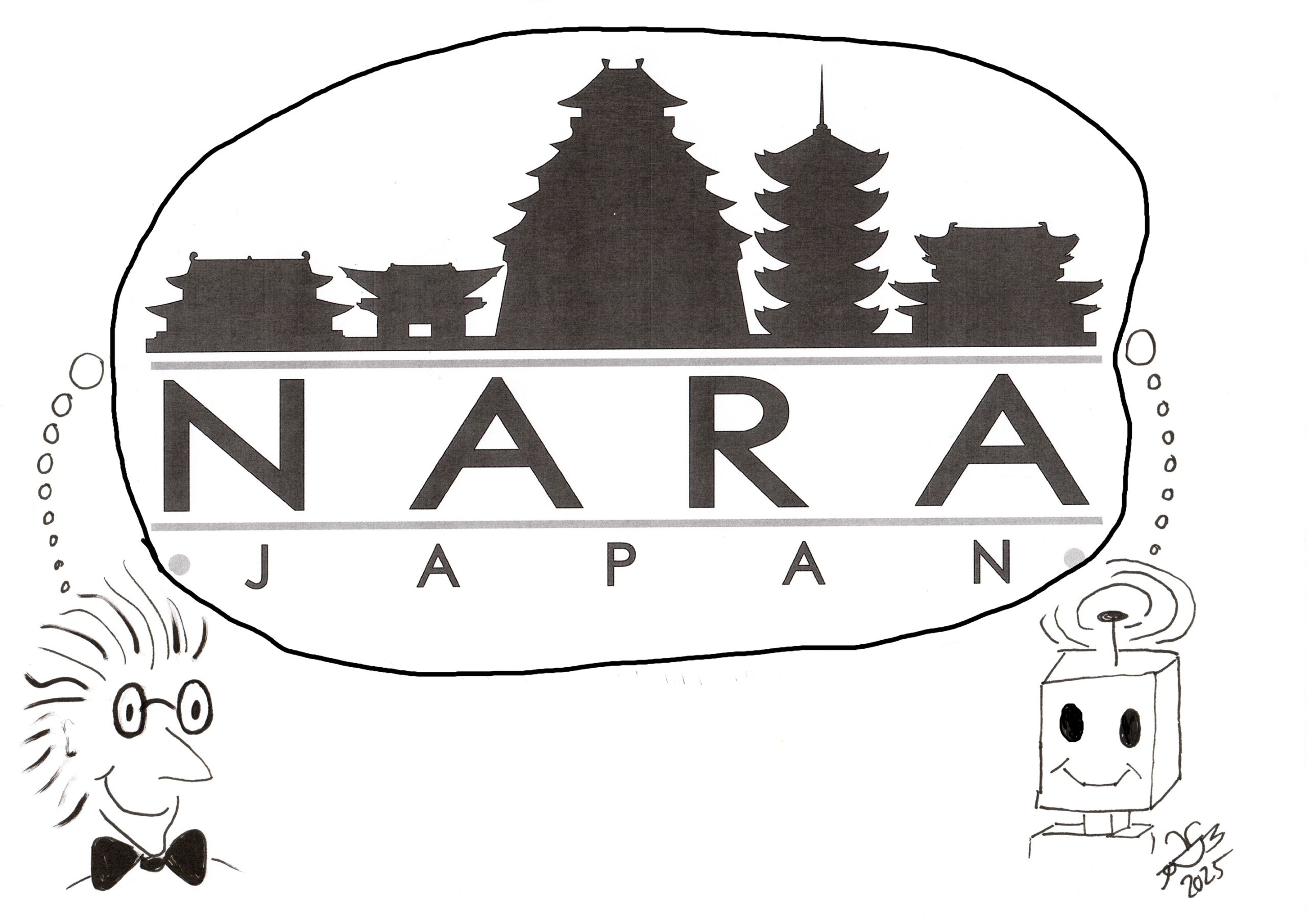
NanoWorld AG CEO Manfred Detterbeck will be at the NanoAndMore Japan booth at the 63rd Annual Meeting of the Biophysical Society of Japan held from September 24– 26, 2025 at Nara Prefectural Convention Center. Will we meet you there too?
Skyline of Nara
JosepPerianes/Shutterstock.com