Phonon polaritons (PhPs) have attracted significant interest in the nano-optics communities because of their nanoscale confinement and long lifetimes. Although PhP modification by changing the local dielectric environment has been reported, controlled manipulation of PhPs by direct modification of the polaritonic material itself has remained elusive.*
In the article “Chemical switching of low-loss phonon polaritons in α-MoO3 by hydrogen intercalation” Yingjie Wu, Qingdong Ou, Yuefeng Yin, Yun Li, Weiliang Ma, Wenzhi Yu, Guanyu Liu, Xiaoqiang Cui, Xiaozhi Bao, Jiahua Duan, Gonzalo Álvarez-Pérez, Zhigao Dai, Babar Shabbir, Nikhil Medhekar, Xiangping Li, Chang-Ming Li, Pablo Alonso-González and Qiaoliang Bao demonstrate an effective chemical approach to manipulate PhPs in α-MoO3 by the hydrogen intercalation-induced perturbation of lattice vibrations.*
Their methodology establishes a proof of concept for chemically manipulating polaritons, offering opportunities for the growing nanophotonics community.*
The surface topography and near-field images presented in this article were captured using a commercial s-SNOM setup with a platinum iridium coated NanoWorld Arrow-NCPt AFM probe in tapping mode.*
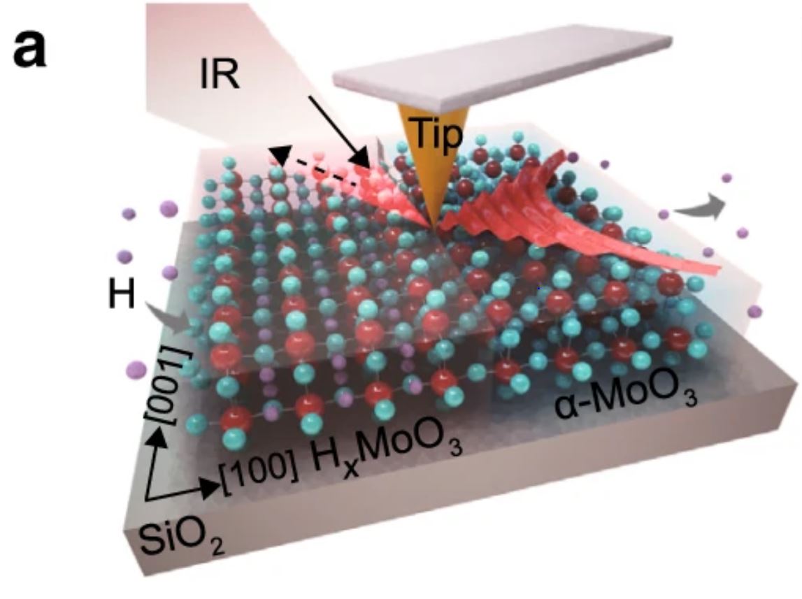
Reversible switching of PhPs in the L-RB of α-MoO3 a Schematic of the s-SNOM measurement and PhP propagation in a typical H-MoO3/α-MoO3 in-plane heterostructure.
2 a Schematic of the s-SNOM measurement and PhP propagation in a typical H-MoO3/α-MoO3 in-plane heterostructure. Please follow this external link for the full figure: https://www.nature.com/articles/s41467-020-16459-3/figures/2
*Yingjie Wu, Qingdong Ou, Yuefeng Yin, Yun Li, Weiliang Ma, Wenzhi Yu, Guanyu Liu, Xiaoqiang Cui, Xiaozhi Bao, Jiahua Duan, Gonzalo Álvarez-Pérez, Zhigao Dai, Babar Shabbir, Nikhil Medhekar, Xiangping Li, Chang-Ming Li, Pablo Alonso-González & Qiaoliang Bao
Chemical switching of low-loss phonon polaritons in α-MoO3 by hydrogen intercalation
Nature Communications volume 11, Article number: 2646 (2020)
DOI: https://doi.org/10.1038/s41467-020-16459-3
Please follow this external link to read the full article https://rdcu.be/b46eT
Open Access The article “ Chemical switching of low-loss phonon polaritons in α-MoO3 by hydrogen intercalation “ by Yingjie Wu, Qingdong Ou, Yuefeng Yin, Yun Li, Weiliang Ma, Wenzhi Yu, Guanyu Liu, Xiaoqiang Cui, Xiaozhi Bao, Jiahua Duan, Gonzalo Álvarez-Pérez, Zhigao Dai, Babar Shabbir, Nikhil Medhekar, Xiangping Li, Chang-Ming Li, Pablo Alonso-González and Qiaoliang Bao is licensed under a Creative Commons Attribution 4.0 International License, which permits use, sharing, adaptation, distribution and reproduction in any medium or format, as long as you give appropriate credit to the original author(s) and the source, provide a link to the Creative Commons license, and indicate if changes were made. The images or other third party material in this article are included in the article’s Creative Commons license, unless indicated otherwise in a credit line to the material. If material is not included in the article’s Creative Commons license and your intended use is not permitted by statutory regulation or exceeds the permitted use, you will need to obtain permission directly from the copyright holder. To view a copy of this license, visit http://creativecommons.org/licenses/by/4.0/.

