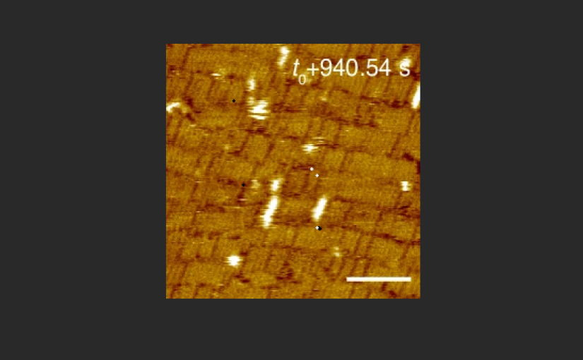
How the surface beneath a protein can influence the structures it forms
What determines whether nanoscale building blocks assemble into an ordered structure or remain disordered?
In a study published in Nature Communications, Sakshi Yadav Schmid and colleagues investigated this question using designed protein nanorods at liquid–solid interfaces. Combining high-speed atomic force microscopy (HS-AFM), machine-learning analysis and computational modelling, they explored how the surface beneath the proteins influences their movement and organization.
The researchers observed a striking contrast: the same protein nanorods formed different arrangements on two types of mica, even though both surfaces have the same potassium-ion sublattice to which the proteins were designed to bind. Their findings reveal why understanding nanoscale assembly requires looking beyond the interactions deliberately built into the protein design.
Following protein assembly in real time
Self-assembly occurs when individual building blocks organize into larger structures through interactions with one another and their surroundings. To understand how these structures form, it helps to observe the process as it unfolds—not just examine the final arrangement.
High-speed AFM allowed the researchers to observe the protein nanorods in liquid as the assembly process unfolded. Using NanoWorld ARROW-UHFAuD and USC-F1.2-k0.15 cantilevers in their high-speed AFM experiments, they could follow how the nanorods moved and how their arrangements changed over time, rather than relying solely on images of the final structures.
The experiments compared two substrates: muscovite mica (m-mica) and fluorophlogopite mica (f-mica). Under the high-salt conditions investigated, the nanorods behaved very differently on the two surfaces.
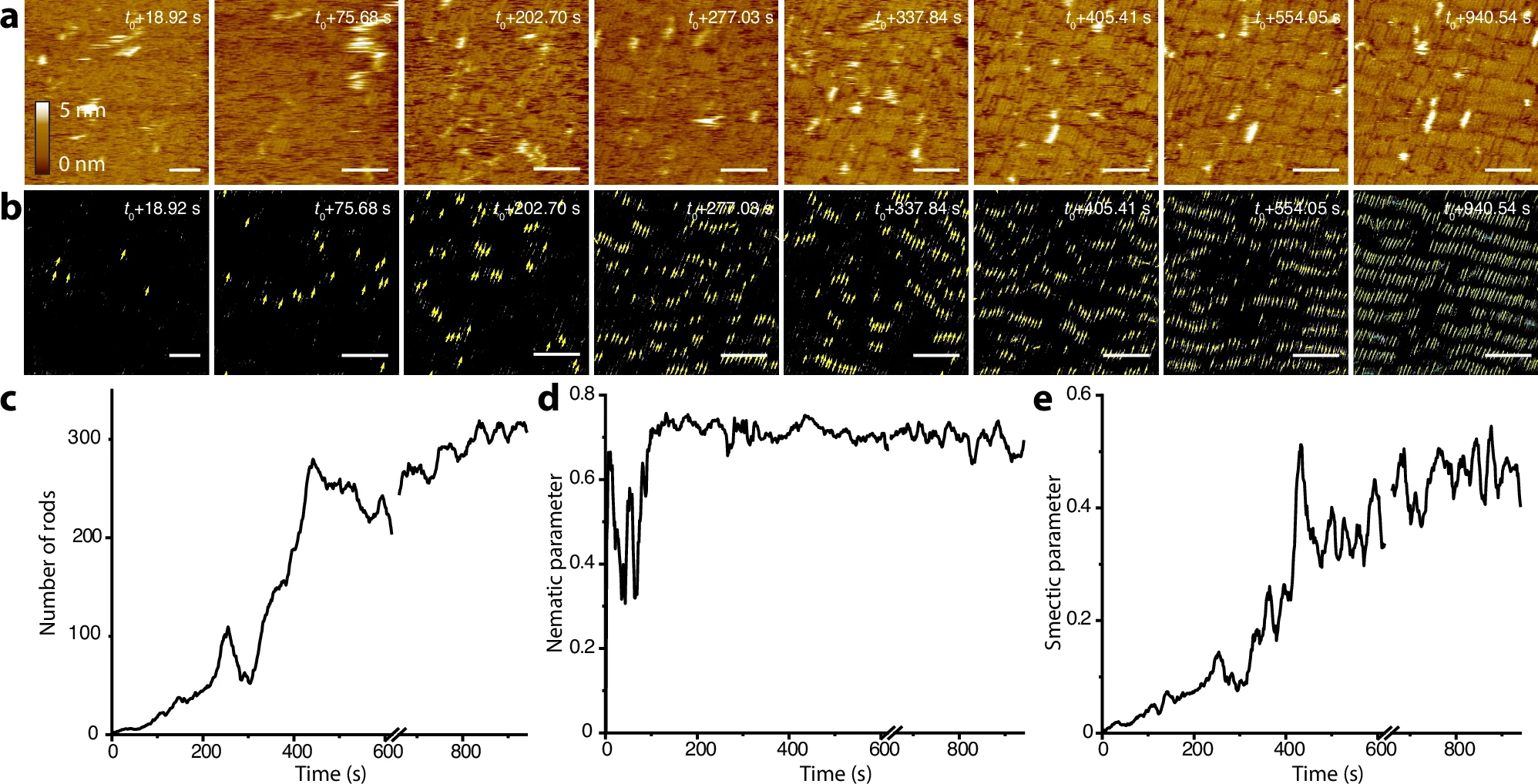
On muscovite mica, the nanorods were highly mobile. Small groups of aligned rods appeared, grew and rearranged until a more stable, layered structure emerged. This arrangement is known as smectic order: the elongated building blocks point predominantly in the same direction and are organized into layers.
Source: Yadav Schmid et al., Nature Communications 17, 2446 (2026), https://doi.org/10.1038/s41467-026-69170-0. © Battelle Memorial Institute and The Authors 2026. Licensed under CC BY 4.0. Reproduced without modification.
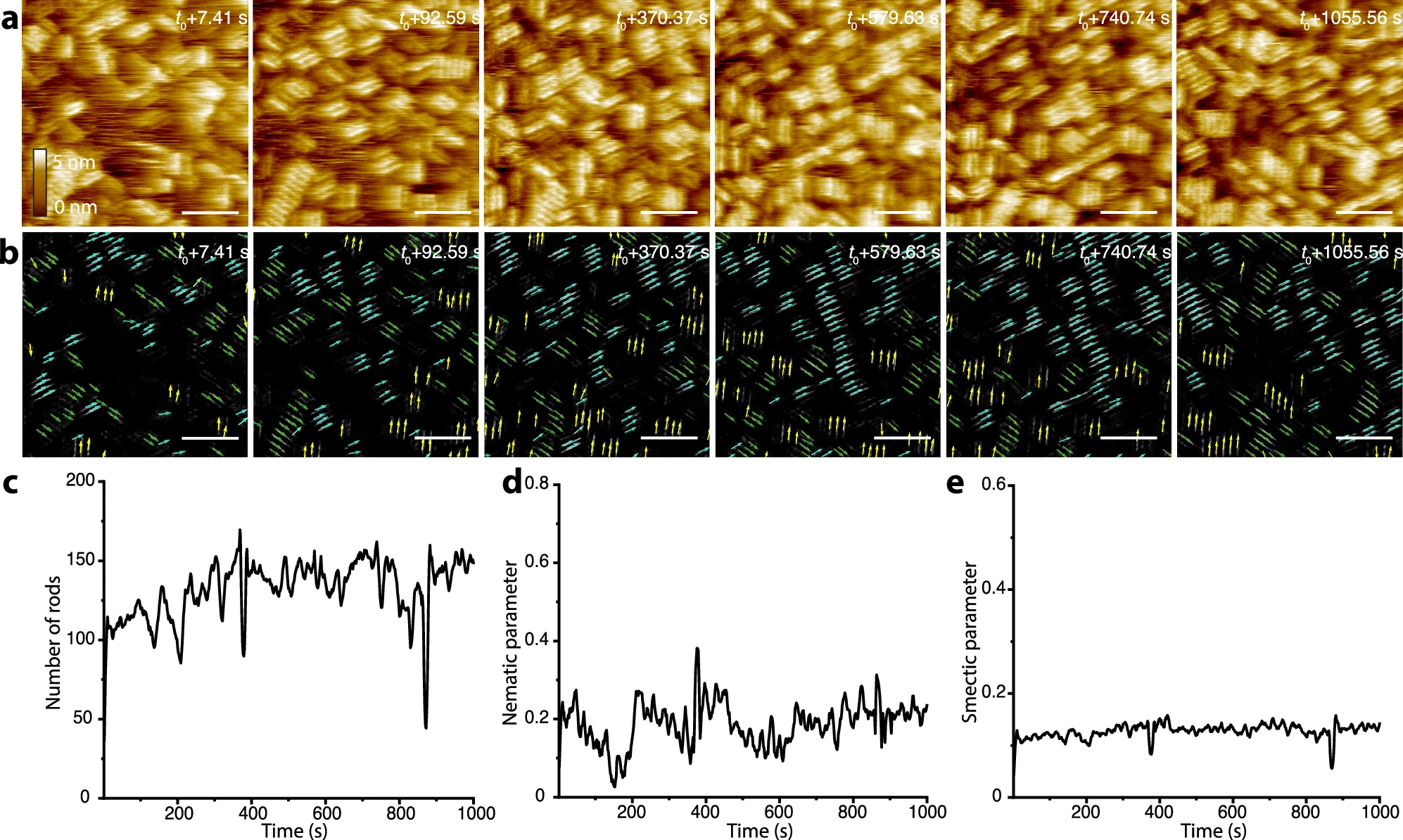
On fluorophlogopite mica, the rods showed translational and rotational movement but were less mobile overall. Their orientations followed three directions associated with the substrate’s potassium-ion sublattice. As more rods accumulated, they formed a high-density disordered assembly, rather than the layered structure seen on muscovite mica.
Source: Yadav Schmid et al., Nature Communications 17, 2446 (2026), https://doi.org/10.1038/s41467-026-69170-0. © Battelle Memorial Institute and The Authors 2026. Licensed under CC BY 4.0. Reproduced without modification.
The difference was particularly intriguing because the potassium-ion patterns that guide protein binding are identical on the two substrates. Something beyond that shared pattern was influencing the outcome.
Measuring how order develops
Watching nanorods move provides a view of self-assembly in action. But how can researchers measure the transition from individual movements to collective organization?
The team used machine-learning methods to identify nanorods in the high-speed AFM images and determine their positions and orientations. From these measurements, they could track surface coverage and calculate how the degree of order changed over time.
Two quantities were especially useful. Nematic order describes how strongly elongated objects align in a common direction. Smectic order additionally captures their organization into layers.
On muscovite mica, the nanorods aligned relatively quickly, while their layered organization developed more gradually as surface coverage increased. On fluorophlogopite mica, the rods accumulated without developing comparable long-range alignment or smectic order.
This quantitative analysis showed not only that the final structures differed, but also how the two assembly processes followed different paths.
Why the surface matters
What could explain such different behavior on substrates with identical potassium-ion sublattices?
An important clue lies in the water next to the solid surface. The atomic structures of muscovite and fluorophlogopite mica differ in ways that influence the arrangement of nearby water molecules. These interfacial hydration structures can, in turn, affect the interactions experienced by the protein nanorods.
To investigate this explanation, the researchers used Monte Carlo simulations that considered the mobility of rod-shaped building blocks and the influence of preferred orientations imposed by the substrate. When the model introduced a directional preference representing the broken symmetry associated with muscovite mica, smectic ordering could emerge. Without that preference, the model reproduced behavior consistent with disordered assembly.
The distinction between the methods is important: high-speed AFM revealed how the nanorods moved and assembled, machine-learning analysis quantified the developing order, and the simulations helped explain how surface-related effects could produce the observed differences.
The findings highlight a factor that is easy to overlook when designing protein assemblies: the surrounding liquid and the structure of the underlying surface can influence the outcome, even when the intended protein–surface binding pattern is the same.
By revealing these effects as assembly happens, high-speed AFM provides an experimental window into processes that may be difficult to understand from finished structures alone. Combined with quantitative analysis and modelling, such observations can help researchers develop a more complete understanding of how designed proteins organize at interfaces.
Full citation
Yadav Schmid, S.; Helfrecht, B.; Stegmann, A.; Legg, B. A.; Pyles, H.; Chen, J.; Edison, J. R.; Ziatdinov, M.; Preisler, Z.; Dollar, O.; Whitelam, S.; Kalinin, S.; Baker, D.; Mundy, C. J.; Zhang, S.; De Yoreo, J. J.
Impact of solvent forces and broken symmetry on the assembly of designed proteins at a liquid-solid interface.
Nature Communications 2026, 17, 2446.
https://doi.org/10.1038/s41467-026-69170-0
Creative Commons Attribution 4.0 International (CC BY 4.0)