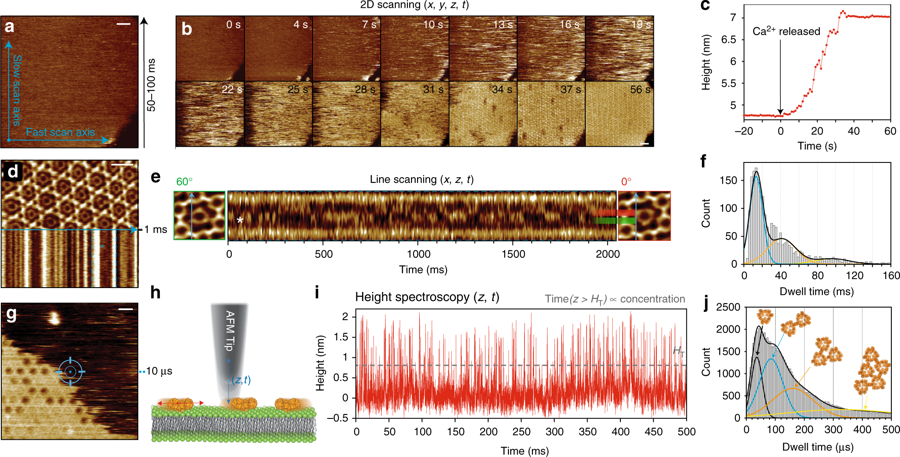
In their recent publication “High-speed AFM height spectroscopy reveals μs-dynamics of unlabeled biomolecules” in Nature Communications George R. Heath and Simon Sheuring develop and apply HS-AFM height spectroscopy (HS-AFM-HS, a technique inspired by fluorescence spectroscopy), a technique whereby the AFM tip is held at a fixed x–y position and the height fluctuations under the tip in z-direction with Angstrom spatial and 10µs temporal resolution are monitored.
They demonstrate “how this technique can be used to simultaneously measure surface concentrations, diffusion rates and oligomer sizes of highly mobile annexin-V molecules during membrane-binding and self-assembly at model membranes and derive its kinetic and energetic terms. Additionally, HS-AFM-HS at specific positions in the annexin lattice where the freedom of movement is restricted to rotation allowed determination of the interaction free energies of protein-protein contacts.”* The applicability of this technique is wide and is discussed at the end of the publication.
NanoWorld Ultra-Short Cantilevers (USC) for Fast-/High-Speed AFM ( USC-F1.2-k0.15 ) were used.
Congratulations to the authors to this publication which pushes the speed limits of AFM even further!
*George R. Heath & Simon Scheuring
High-speed AFM height spectroscopy reveals μs-dynamics of unlabeled biomolecules
Nature Communicationsvolume 9, Article number: 4983 (2018)
DOI: https://doi.org/10.1038/s41467-018-07512-3
Please follow this external link for the full article: https://rdcu.be/bdaKU
Open Access The article “High-speed AFM height spectroscopy reveals μ s-dynamics of unlabeled biomolecules” by George R. Heath & Simon Scheuring is licensed under a Creative Commons Attribution 4.0 International License, which permits use, sharing, adaptation, distribution and reproduction in any medium or format, as long as you give appropriate credit to the original author(s) and the source, provide a link to the Creative Commons license, and indicate if changes were made. The images or other third party material in this article are included in the article’s Creative Commons license, unless indicated otherwise in a credit line to the material. If material is not included in the article’s Creative Commons license and your intended use is not permitted by statutory regulation or exceeds the permitted use, you will need to obtain permission directly from the copyright holder. To view a copy of this license, visit http://creativecommons.org/licenses/by/4.0/.