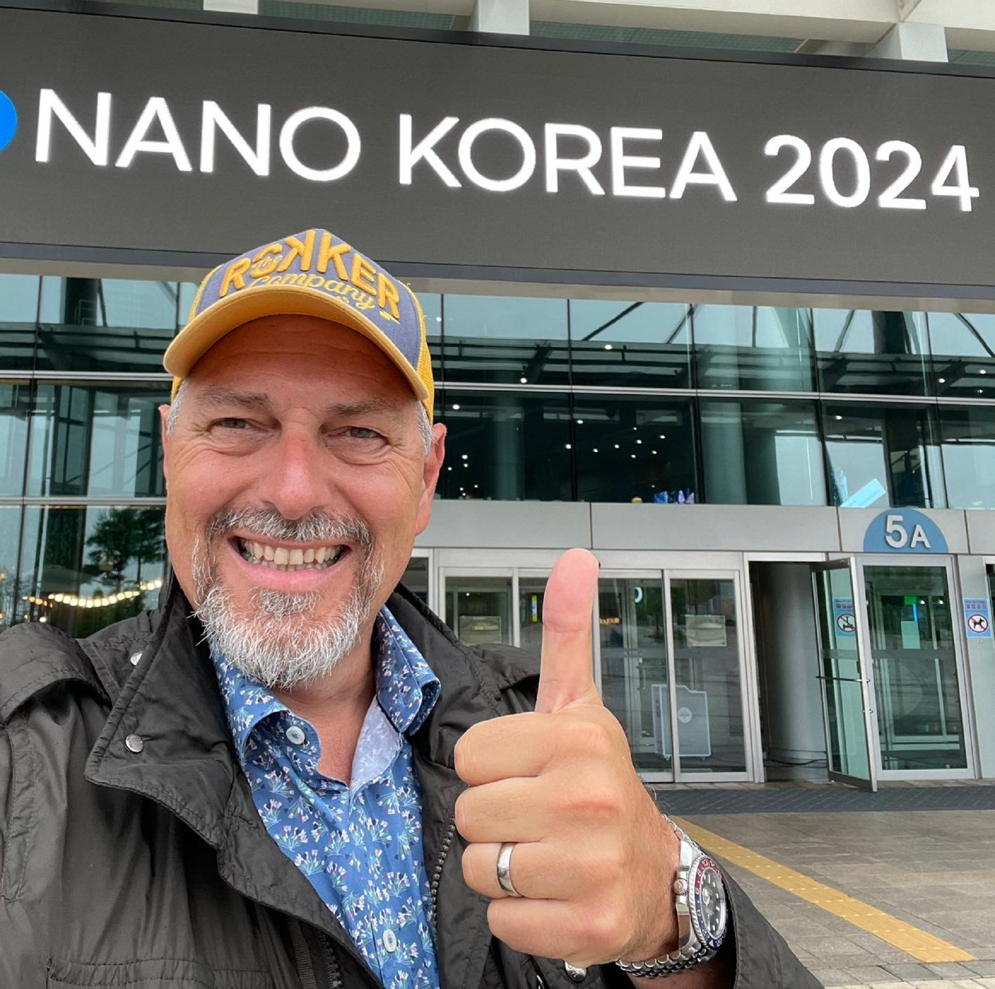
Atomistic insights into highly active reconstructed edges of monolayer 2H-WSe 2 photocatalyst

Today, October 9, 2022, is National #NanotechnologyDay in the US. The theme for this year’s National Nanotechnology Day is nanotechnology’s role in understanding and responding to climate change and improving the health of the Earth and its people.

Climate change has necessitated the framing of government regulations and the development of green strategies for reducing CO2 emissions. Scientists worldwide are engaged in efforts to find sustainable solutions to the problem of CO2 level in the air.*

Ascertaining the function of in-plane intrinsic defects and edge atoms is necessary for developing efficient low-dimensional photocatalysts.*

In their article “Atomistic insights into highly active reconstructed edges of monolayer 2H-WSe 2 photocatalyst” Mohammad Qorbani , Amr Sabbah, Ying-Ren Lai, Septia Kholimatussadiah, Shaham Quadir , Chih-Yang Huang, Indrajit Shown, Yi-Fan Huang, Michitoshi Hayashi, Kuei-Hsien Chen and Li-Chyong Chen report the wireless photocatalytic CO2 reduction to CH4 over reconstructed edge atoms of monolayer 2H-WSe2 artificial leaves.*

Their first-principles calculations demonstrate that reconstructed and imperfect edge configurations enable CO2 binding to form linear and bent molecules. Experimental results show that the solar-to-fuel quantum efficiency is a reciprocal function of the flake size. It also indicates that the consumed electron rate per edge atom is two orders of magnitude larger than the in-plane intrinsic defects. Further, nanoscale redox mapping at the monolayer WSe2–liquid interface confirms that the edge is the most preferred region for charge transfer.*

The author’s results pave the way for designing a new class of monolayer transition metal dichal-cogenides with reconstructed edges as a non-precious co-catalyst for wired or wireless hydrogen evolution or CO2 reduction reactions.*

The thickness of the WSe 2 flake was measured by using Atomic Force Microscopy with a NanoWorld Pointprobe® NCHR AFM probe and was controlled by a feedback mechanism. The AFM cantilever was driven under a resonant frequency of ~330 kHz and 42 N m−1 spring constant.*

Figure 4 from “Atomistic insights into highly active reconstructed edges of monolayer 2H-WSe2 photocatalyst” by Mohammad Qorbani et al: Nanoscale redox mapping and PC performance a FE-SEM image of the ML WSe2 in dark (control experiment) in the solution containing Ag ions. b FE-SEM images of the ML WSe2 under light after Ag photodeposition for 1 h, respectively. Bright regions show the presence of Ag nanoparticles. Inset illustrates the photoreduction mechanism. Scale bar = 2 μm. c–e AFM height profile measured in the liquid environment, background normalized SECM feedbacks maps for main, and lift scans, respectively. Scale bar = 1 μm. f Color map of the blank-corrected total methane yield as a function of flake sizes (in perimeters) and areas. g Blank-corrected IQE as a function of the average flake perimeter. The black line shows the fitted reciprocal curve. h Stability test for six cycles. Irradiation time for each cycle is 4 h. NanoWorld Pointprobe NCHR AFM probes were used for the atomic force microscopy
Figure 4 from “Atomistic insights into highly active reconstructed edges of monolayer 2H-WSe2 photocatalyst” by Mohammad Qorbani et al:
Nanoscale redox mapping and PC performance
a FE-SEM image of the ML WSe2 in dark (control experiment) in the solution containing Ag ions. b FE-SEM images of the ML WSe2 under light after Ag photodeposition for 1 h, respectively. Bright regions show the presence of Ag nanoparticles. Inset illustrates the photoreduction mechanism. Scale bar = 2 μm. c–e AFM height profile measured in the liquid environment, background normalized SECM feedbacks maps for main, and lift scans, respectively. Scale bar = 1 μm. f Color map of the blank-corrected total methane yield as a function of flake sizes (in perimeters) and areas. g Blank-corrected IQE as a function of the average flake perimeter. The black line shows the fitted reciprocal curve. h Stability test for six cycles. Irradiation time for each cycle is 4 h.

*Mohammad Qorbani , Amr Sabbah, Ying-Ren Lai, Septia Kholimatussadiah, Shaham Quadir , Chih-Yang Huang, Indrajit Shown, Yi-Fan Huang, Michitoshi Hayashi, Kuei-Hsien Chen and Li-Chyong Chen
Atomistic insights into highly active reconstructed edges of monolayer 2H-WSe 2 photocatalyst
Nature communications (2022) 13:1256
DOI:  https://doi.org/10.1038/s41467-022-28926-0

Please follow this external link to read the full article: https://rdcu.be/cXbA6

Open Access
The article “Atomistic insights into highly active reconstructed edges of monolayer 2H-WSe 2 photocatalyst” by Mohammad Qorbani , Amr Sabbah, Ying-Ren Lai, Septia Kholimatussadiah, Shaham Quadir , Chih-Yang Huang, Indrajit Shown, Yi-Fan Huang, Michitoshi Hayashi, Kuei-Hsien Chen and Li-Chyong Chen is licensed under a Creative Commons Attribution 4.0 International License, which permits use, sharing, adaptation, distribution and reproduction in any medium or format, as long as you give appropriate credit to the original author(s) and the source, provide a link to the Creative Commons license, and indicate if changes were made. The images or other third party material in this article are included in the article’s Creative Commons license, unless indicated otherwise in a credit line to the material. If material is not included in the article’s Creative Commons license and your intended use is not permitted by statutory regulation or exceeds the permitted use, you will need to obtain permission directly from the copyright holder. To view a copy of this license, visit http://creativecommons.org/licenses/by/4.0/.

Influence of B/N co-doping on electrical and photoluminescence properties of CVD grown homoepitaxial diamond films

Boron doped diamond (BDD) has great potential in electrical, and electrochemical sensing applications. The growth parameters, substrates, and synthesis method play a vital role in the preparation of semiconducting BDD to metallic BDD. Doping of other elements along with boron (B) into diamond demonstrated improved efficacy of B doping and exceptional properties.*

In the article “Influence of B/N co-doping on electrical and photoluminescence properties of CVD grown homoepitaxial diamond films” Srinivasu Kunuku, Mateusz Ficek, Aleksandra Wieloszynska, Magdalena Tamulewicz-Szwajkowska, Krzysztof Gajewski, Miroslaw Sawczak, Aneta Lewkowicz, Jacek Ryl, Tedor Gotszalk and Robert Bogdanowicz describe how B and nitrogen (N) co-doped diamond has been synthesized on single crystalline diamond (SCD) IIa and SCD Ib substrates in a microwave plasma-assisted chemical vapor deposition process.*

The surface topography of the CVD diamond layers was investigated using atomic force microscopy (AFM), and Kelvin probe force microscopy (KPFM) was employed to measure the contact potential difference (CPD) to calculate the work function of these CVD diamond layers.*

Atomic force microscopy topography depicted the flat and smooth surface with low surface roughness for low B doping, whereas surface features like hillock structures and un-epitaxial diamond crystals with high surface roughness were observed for high B doping concentrations. KPFM measurements revealed that the work function (4.74–4.94 eV) has not varied significantly for CVD diamond synthesized with different B/C concentrations.*

NanoWorld ARROW-EFM conductive platinumirdidium5 coated AFM probes with a typical spring constant of 2.8 N/m and a typical resonant frequency of 75 kHz were used.*

Figure 2 from “Influence of B/N co-doping on electrical and photoluminescence properties of CVD grown homoepitaxial diamond films “ by Srinivasu Kunuku et al: AFM topography of B/N co-doped CVD diamond on (with fixed N/C = 0.02) SCD IIa; (a) B/C ∼ 2500 ppm (b) B/C ∼ 5000 ppm (c) B/C ∼ 7500 ppm, and KPFM CPD images of B/N co-doped CVD diamond (with fixed N/C = 0.02) on SCD IIa; (d) B/C ∼ 2500 ppm (e) B/C ∼ 5000 ppm (f) B/C ∼ 7500 ppm. NanoWorld Arrow-EFM platinumiridium coated AFM probes were used for the KPFM and surface topography measurements.
Figure 2 from “Influence of B/N co-doping on electrical and photoluminescence properties of CVD grown homoepitaxial diamond films “ by Srinivasu Kunuku et al:
AFM topography of B/N co-doped CVD diamond on (with fixed N/C = 0.02) SCD IIa; (a) B/C ∼ 2500 ppm (b) B/C ∼ 5000 ppm (c) B/C ∼ 7500 ppm, and KPFM CPD images of B/N co-doped CVD diamond (with fixed N/C = 0.02) on SCD IIa; (d) B/C ∼ 2500 ppm (e) B/C ∼ 5000 ppm (f) B/C ∼ 7500 ppm.

*Srinivasu Kunuku, Mateusz Ficek, Aleksandra Wieloszynska, Magdalena Tamulewicz-Szwajkowska, Krzysztof Gajewski, Miroslaw Sawczak, Aneta Lewkowicz, Jacek Ryl, Tedor Gotszalk and Robert Bogdanowicz
Influence of B/N co-doping on electrical and photoluminescence properties of CVD grown homoepitaxial diamond films
Nanotechnology (2022),  33 125603
DOI: https://doi.org/10.1088/1361-6528/ac4130

Please follow this external link to read the full article: https://doi.org/10.1088/1361-6528/ac4130

Open Access The article “Influence of B/N co-doping on electrical and photoluminescence properties of CVD grown homoepitaxial diamond films” by Srinivasu Kunuku, Mateusz Ficek, Aleksandra Wieloszynska, Magdalena Tamulewicz-Szwajkowska, Krzysztof Gajewski, Miroslaw Sawczak, Aneta Lewkowicz, Jacek Ryl, Tedor Gotszalk and Robert Bogdanowicz is licensed under a Creative Commons Attribution 4.0 International License, which permits use, sharing, adaptation, distribution and reproduction in any medium or format, as long as you give appropriate credit to the original author(s) and the source, provide a link to the Creative Commons license, and indicate if changes were made. The images or other third party material in this article are included in the article’s Creative Commons license, unless indicated otherwise in a credit line to the material. If material is not included in the article’s Creative Commons license and your intended use is not permitted by statutory regulation or exceeds the permitted use, you will need to obtain permission directly from the copyright holder. To view a copy of this license, visit http://creativecommons.org/licenses/by/4.0/.