Eom S, Kavle P, Kang D, Kim Y, Martin LW, Hong S
Unveiling the Nanoscale Dielectric Gap and Its Influence on Ferroelectric Polarization Switching in Scanning Probe Microscopy
Advanced Functional Materials. 2025 Mar;35(11):2406944
DOI: https://doi.org/10.1002/adfm.202406944
Kapustić K, G. Ayani C, Pielić B, Plevová K, Mandić S, Šrut Rakić I
Visualizing Intercalation Effects in 2D Materials Using AFM-Based Techniques
The Journal of Physical Chemistry Letters. 2025 May 7;16(19):4804-11
DOI: https://doi.org/10.1021/acs.jpclett.5c00322
Seredin P, Goloshchapov D, Emelyanova A, Eremeev K, Peshkov Y, Shikhaliev K, Potapov A, Ippolitov Y, Kashkarov V, Nesterov D, Shapiro K
Rapid Deposition of the Biomimetic Hydroxyapatite-Polydopamine-Amino Acid Composite Layers onto the Natural Enamel
ACS omega. 2024 Apr 8;9(15):17012-27
DOI: https://doi.org/10.1021/acsomega.3c08491
Zhang M, Guo Z, Gellman AJ, Salvador PA, Rohrer GS
Influence of the molten SrCl2 treatment on the surface structure and photochemical reactivities of SrTiO3
Applied Surface Science. 2023 Nov 30;638:158111
DOI: https://doi.org/10.1016/j.apsusc.2023.158111
Senkić A, Bajo J, Supina A, Radatović B, Vujičić N
Effects of CVD growth parameters on global and local optical properties of MoS2 monolayers
Materials chemistry and physics. 2023 Feb 15;296:127185
DOI: https://doi.org/10.1016/j.matchemphys.2022.127185
Izumi R, Miyazaki M, Li YJ, Sugawara Y
High–low Kelvin probe force spectroscopy for measuring the interface state density
Beilstein Journal of Nanotechnology. 2023 Jan 31;14(1):175-89
DOI: https://doi.org/10.3762/bjnano.14.18
Zhou Z, Wang S, Zhou Z, Hu Y, Li Q, Xue J, Feng Z, Yan Q, Luo Z, Weng Y, Tang R.
Unconventional polarization fatigue in van der Waals layered ferroelectric ionic conductor CuInP2S6
Nature Communications. 2023 Dec 12;14(1):8254
DOI: https://doi.org/10.1038/s41467-023-44132-y
Liu C, Shviro M, Gago AS, Zaccarine SF, Bender G, Gazdzicki P, Morawietz T, Biswas I, Rasinski M, Everwand A, Schierholz R
Exploring the Interface of skin‐layered titanium fibers for electrochemical water splitting
Advanced Energy Materials. 2021 Feb;11(8):2002926
DOI: https://doi.org/10.1002/aenm.202002926
Zhou S, You L, Chaturvedi A, Morris SA, Herrin JS, Zhang N, Abdelsamie A, Hu Y, Chen J, Zhou Y, Dong S
Anomalous polarization switching and permanent retention in a ferroelectric ionic conductor
Materials Horizons. 2020;7(1):263-74
DOI: https://doi.org/10.1039/C9MH01215J
Moro D, Ulian G, Valdrè G
3D meso-nanostructures in cleaved and nanolithographed Mg-Al-hydroxysilicate (clinochlore): Topology, crystal-chemistry, and surface properties
Applied Clay Science. 2019 Mar 1;169:74-80
DOI: https://doi.org/10.1016/j.clay.2018.12.020
Otsuka Y, Nishijima S, Sakamoto L, Kajimoto K, Araki K, Misaka T, Ohoyama H, Matsumoto T
Chemical Control of Electronic Coupling between a Ruthenium Complex and Gold Electrode for Resonant Tunneling Conduction
Materials & Interfaces. 2019 Jun 6;11(27):24331-8
DOI: https://doi.org/10.1021/acsami.9b05569
Wang H, Zeng K
Domain structure, local surface potential distribution and relaxation of Pb (Zn1/3Nb2/3) O3–9% PbTiO3 (PZN–9% PT) single crystals
Journal of Materiomics. 2016 Dec 1;2(4):309-15
DOI: https://doi.org/10.1016/j.jmat.2016.08.001
Kawasaki S, Takahashi R, Yamamoto T, Kobayashi M, Kumigashira H, Yoshinobu J, Komori F, Kudo A, Lippmaa M
Photoelectrochemical water splitting enhanced by self-assembled metal nanopillars embedded in an oxide semiconductor photoelectrode
Nature communications. 2016 Jun 3;7(1):11818
DOI: https://doi.org/10.1038/ncomms11818
Moro D, Ulian G, Valdre G
Single molecule investigation of glycine–chlorite interaction by cross-correlated scanning probe microscopy and quantum mechanics simulations
Langmuir. 2015 Apr 21;31(15):4453-63
DOI: https://doi.org/10.1021/acs.langmuir.5b00161
Stevanović V, Hartman K, Jaramillo R, Ramanathan S, Buonassisi T, Graf P.
Variations of ionization potential and electron affinity as a function of surface orientation: The case of orthorhombic SnS
Applied Physics Letters. 2014 May 26;104(21).
DOI: https://doi.org/10.1063/1.4879558
Valdre G, Moro D
Radiofrequency impedance variation of characterized tip–sample nanocontacts in shear force microscopy with vertically oriented cantilevers connected to a vector network analyser
Measurement Science and Technology. 2013 Jul 26;24(9):095901
DOI: https://doi.org/10.1088/0957-0233/24/9/095901
Matsuda M, Kinoshita N, Fujishima M, Tanaka S, Tajima H, Hasegawa H
Electrochemically Fabricated Phthalocyanine-Based Molecular Conductor Films and Their Potential Use in Organic Electronic Devices
Applied Physics Express. 2013 Feb 5;6(2):021602
DOI: https://doi.org/10.7567/APEX.6.021602
Valdre G, Tosoni S, Moro D
Zeolitic-type Brønsted-Lowry sites distribution imaged on clinochlore
American Mineralogist. 2011 Oct 1;96(10):1461-6
DOI: https://doi.org/10.2138/am.2011.3774
Li T, Zeng K
Piezoelectric properties and surface potential of green abalone shell studied by scanning probe microscopy techniques
Acta Materialia. 2011 May 1;59(9):3667-79
DOI: https://doi.org/10.1016/j.actamat.2011.03.001
Wong MF, Zeng K
Nanoscale domains and preferred cracking planes in Pb (Zn1/3Nb2/3) O3–(6–7)% PbTiO3 single crystals studied by piezoresponse force microscopy and fractography
Journal of Applied Physics. 2010 Jun 15;107(12)
DOI: https://doi.org/10.1063/1.3452330
Valdrè G, Malferrari D, Brigatti MF
Crystallographic features and cleavage nanomorphology of chlinochlore: specific applications
Clays and clay minerals. 2009 Apr 1;57(2):183-93
DOI: https://doi.org/10.1346/CCMN.2009.0570205
Tsutsumi JY, Yoshida H, Murdey R, Sato N
Spontaneous buildup of surface potential with a thin film of a zwitterionic molecule giving noncentrosymmetric crystal structure
Applied Physics Letters. 2009 Nov 2;95(18)
DOI: https://doi.org/10.1063/1.3254217


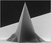
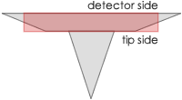 A trapezoidal cross section of the AFM cantilever and therefore 30% wider (e.g. NCH) AFM cantilever detector side result in easier and faster laser adjustment. Additionally, because there is simply more space to place and reflect the laser beam, a higher SUM signal is reached.

 POINTPROBE®
 ARROW™
 ULTRA-SHORT CANTILEVERS
 PYREX-NITRIDE
 COATINGS