In the last decades enormous advances have been made in characterizing the atomic and molecular structure of respiratory chain supercomplexes. *
However, it still remains a challenge to stitch this refined spatial atomistic description with functional information provided by biochemical studies of isolated protein material. Development of functional assays that detect respiratory chain complexes in their native membrane environment contribute to address the open questions related to the role played by their association and interactions. *
In the article “Electrochemical detection of quinone reduced by Complex I Complex II and Complex III in full mitochondrial membranes” Daniel G. Cava, Julia Alvarez-Malmagro, Paolo Natale, Sandra López-Calcerrada, Iván López-Montero, Cristina Ugalde, Jose Maria Abad, Marcos Pita, Antonio L. De Lacey and Marisela Vélez present a characterization assay in which a functionalized gold electrode is modified with mitochondrial membrane fragments that allows monitoring electrochemically the activity of different respiratory chain complexes immersed in the mitochondrial membrane. *
Daniel G. Cava et al. measure the intensity of the reducing current of the electron mediator CoQ1 at the electrode surface and its variation upon addition of the corresponding enzymatic substrates. The activities of Complex I, Complex II and Complex III were monitored by the way in which they reduce the current, reflecting the amount of quinone reduced by the complexes in the presence of their substrates. *
The authors detect that CoQ1H2 produced by Complex I remains partially trapped within the membrane and is more easily oxidized by Complex III or the electrode than the quinone reduced by Complex II. *
Atomic Force Microscopy (AFM) was used to image the topography of the membrane modified electrode. NanoWorld Pyrex-Nitride Silicon-Nitride AFM probes (PNP-DB, diving board shaped cantilevers, the short AFM cantilever with a typical force constant of 0.48 N/m and 67 kHz resonance frequency) were used. *
The surfaces analysed were the electrodes. The two surfaces imaged are the same previously polished electrodes used for electrochemical measurements. The microscope sample holder was adapted in-home to support the electrodes. Two surfaces were analysed: the polished gold functionalized with 4-aminothiophenol and the electrode after incubation with mitochondria subparticles prepared similarly to the electrodes used for the electrochemical measurements.*
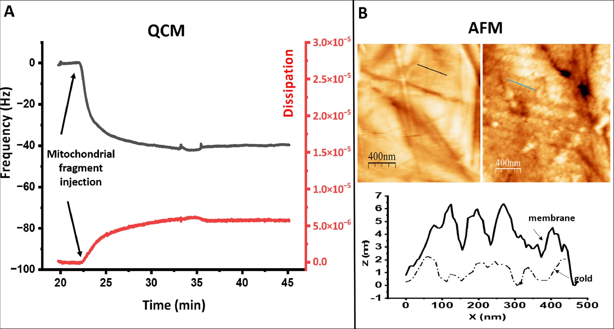
QCM and AFM characterization of modified gold. Panel A shows the frequency (left, black) and dissipation (right red) changes detected on a gold covered quartz crystal previously modified with a 4-ATP after injection in the chamber of the mitochondrial fragments at the time point indicated by the thick arrow. Panel B show AFM images of the surface topography of a modified gold electrode before (left) and after (right)incubation with the mitochondrial membrane. The inset below shows the height profile of the lines indicated in the images.
*Daniel G. Cava, Julia Alvarez-Malmagro, Paolo Natale, Sandra López-Calcerrada, Iván López-Montero, Cristina Ugalde, Jose Maria Abad, Marcos Pita, Antonio L. De Lacey and Marisela Vélez
Electrochemical detection of quinone reduced by Complex I Complex II and Complex III in full mitochondrial membranes
Electrochimica Acta, Volume 484, 20 April 2024, 144042
DOI: https://doi.org/10.1016/j.electacta.2024.144042
The article “Electrochemical detection of quinone reduced by Complex I Complex II and Complex III in full mitochondrial membranes” by Daniel G. Cava, Julia Alvarez-Malmagro, Paolo Natale, Sandra López-Calcerrada, Iván López-Montero, Cristina Ugalde, Jose Maria Abad, Marcos Pita, Antonio L. De Lacey and Marisela Vélez is licensed under a Creative Commons Attribution 4.0 International License, which permits use, sharing, adaptation, distribution and reproduction in any medium or format, as long as you give appropriate credit to the original author(s) and the source, provide a link to the Creative Commons license, and indicate if changes were made. The images or other third-party material in this article are included in the article’s Creative Commons license, unless indicated otherwise in a credit line to the material. If material is not included in the article’s Creative Commons license and your intended use is not permitted by statutory regulation or exceeds the permitted use, you will need to obtain permission directly from the copyright holder. To view a copy of this license, visit https://creativecommons.org/licenses/by/4.0/.